74ALVCH16543DGG,11 NXP Semiconductors, 74ALVCH16543DGG,11 Datasheet - Page 2
74ALVCH16543DGG,11
Manufacturer Part Number
74ALVCH16543DGG,11
Description
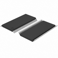
IC TRANSCVR TRI-ST 16BIT 56SSOP
Manufacturer
NXP Semiconductors
Series
74ALVCHr
Datasheet
1.74ALVCH16543DGG11.pdf
(20 pages)
Specifications of 74ALVCH16543DGG,11
Logic Type
Transceiver, Non-Inverting
Number Of Elements
2
Number Of Bits Per Element
8
Current - Output High, Low
24mA, 24mA
Voltage - Supply
1.2 V ~ 3.6 V
Operating Temperature
-40°C ~ 85°C
Mounting Type
Surface Mount
Package / Case
56-TSSOP
Lead Free Status / RoHS Status
Lead free / RoHS Compliant
Other names
74ALVCH16543DG-T
74ALVCH16543DG-T
935262544118
74ALVCH16543DG-T
935262544118


Philips Semiconductors
FEATURES
DESCRIPTION
The 74ALVCH16543 is a dual octal registered transceiver.
Each section contains two sets of D-type latches for
temporary storage of the data flow in either direction.
FUNCTION TABLE
See note 1.
Note
1. XX = AB for A-to-B direction, BA for B-to-A direction;
1999 Nov 23
In accordance with JEDEC standard no 8-1A
CMOS low power consumption
Direct interface with TTL levels
MULTIBYTE
16-bit transceiver with D-type latch
Combines 16245 and 16373 type functions in one chip
Back-to-back registers for storage
Output drive capability 50
Separate controls for data flow in each direction
All data inputs have bus hold
3-state non-inverting outputs for bus oriented
applications
Current drive 24 mA at 3.0 V.
16-bit D-type registered transceiver; 3-state
H = HIGH voltage level; L = LOW voltage level;
h = HIGH state must be present one set-up time before the LOW-to-HIGH transition of nLE
l = LOW state must be present one set-up time before the LOW-to-HIGH transition of nLE
X = don’t care; NC = no change;
Z = high-impedance OFF-state.
nOE
= LOW-to-HIGH level transition;
H
X
L
L
L
L
L
L
L
XX
flow-through pin-out architecture
nE
H
X
L
L
L
L
L
XX
INPUTS
transmission lines at 85 C
nLE
X
X
H
L
L
L
L
XX
nB
n
H
X
X
X
, nA
h
h
L
l
l
n
2
Separate latch enable (nLE
(nOE
permit independent control in either direction of the data
flow.
The ‘16543’ contains two sections each consisting of two
sets of eight D-type latches with separate inputs and
controls for each set. For data flow from A to B, for
example, the A-to-B enable (nE
inputs must be LOW in order to enter data from nA
or take data from nB
table. With nE
enable (nLE
transparent; a subsequent LOW-to-HIGH transition of the
nLE
and nOE
active and display the data present at the output of the
A latches. Similarly, the nE
control the data flow from B-to-A.
Active bus hold circuitry is provided to hold unused or
floating data inputs at a valid logic level.
AB
AB
signal stores the A data into the latches. With nE
, nOE
AB
OUTPUTS
both LOW, the 3-state B output buffers are
AB
BA
AB
NC
) input makes the A-to-B latches
H
H
Z
Z
Z
Z
L
L
) inputs are provided for each register to
LOW, a LOW signal on the A-to-B latch
0
to nB
BA
7
AB
, as indicated in the function
, nLE
, nLE
74ALVCH16543
disabled
disabled
disabled and latch
latch and display
transparent
hold
AB
AB
AB
, where n equals 1 or 2)
BA
, nLE
Product specification
BA
, nLE
) and output enable
and nOE
STATUS
BA
BA
, nE
, nE
AB
BA
AB
0
or nE
signals
or nE
to nA
BA
AB
BA
7
,
;
;
Related parts for 74ALVCH16543DGG,11
Image
Part Number
Description
Manufacturer
Datasheet
Request
R

Part Number:
Description:
NXP Semiconductors designed the LPC2420/2460 microcontroller around a 16-bit/32-bitARM7TDMI-S CPU core with real-time debug interfaces that include both JTAG andembedded trace
Manufacturer:
NXP Semiconductors
Datasheet:

Part Number:
Description:
NXP Semiconductors designed the LPC2458 microcontroller around a 16-bit/32-bitARM7TDMI-S CPU core with real-time debug interfaces that include both JTAG andembedded trace
Manufacturer:
NXP Semiconductors
Datasheet:
Part Number:
Description:
NXP Semiconductors designed the LPC2468 microcontroller around a 16-bit/32-bitARM7TDMI-S CPU core with real-time debug interfaces that include both JTAG andembedded trace
Manufacturer:
NXP Semiconductors
Datasheet:
Part Number:
Description:
NXP Semiconductors designed the LPC2470 microcontroller, powered by theARM7TDMI-S core, to be a highly integrated microcontroller for a wide range ofapplications that require advanced communications and high quality graphic displays
Manufacturer:
NXP Semiconductors
Datasheet:
Part Number:
Description:
NXP Semiconductors designed the LPC2478 microcontroller, powered by theARM7TDMI-S core, to be a highly integrated microcontroller for a wide range ofapplications that require advanced communications and high quality graphic displays
Manufacturer:
NXP Semiconductors
Datasheet:
Part Number:
Description:
The Philips Semiconductors XA (eXtended Architecture) family of 16-bit single-chip microcontrollers is powerful enough to easily handle the requirements of high performance embedded applications, yet inexpensive enough to compete in the market for hi
Manufacturer:
NXP Semiconductors
Datasheet:
Part Number:
Description:
The XA-S3 device is a member of Philips Semiconductors? XA(eXtended Architecture) family of high performance 16-bitsingle-chip microcontrollers
Manufacturer:
NXP Semiconductors
Datasheet:

Part Number:
Description:
The NXP BlueStreak LH75401/LH75411 family consists of two low-cost 16/32-bit System-on-Chip (SoC) devices
Manufacturer:
NXP Semiconductors
Datasheet:
Part Number:
Description:
The NXP LPC3130/3131 combine an 180 MHz ARM926EJ-S CPU core, high-speed USB2
Manufacturer:
NXP Semiconductors
Datasheet:
Part Number:
Description:
The NXP LPC3141 combine a 270 MHz ARM926EJ-S CPU core, High-speed USB 2
Manufacturer:
NXP Semiconductors
Part Number:
Description:
The NXP LPC3143 combine a 270 MHz ARM926EJ-S CPU core, High-speed USB 2
Manufacturer:
NXP Semiconductors

Part Number:
Description:
The NXP LPC3152 combines an 180 MHz ARM926EJ-S CPU core, High-speed USB 2
Manufacturer:
NXP Semiconductors
Part Number:
Description:
The NXP LPC3154 combines an 180 MHz ARM926EJ-S CPU core, High-speed USB 2
Manufacturer:
NXP Semiconductors

Part Number:
Description:
Standard level N-channel enhancement mode Field-Effect Transistor (FET) in a plastic package using NXP High-Performance Automotive (HPA) TrenchMOS technology
Manufacturer:
NXP Semiconductors
Datasheet: