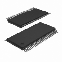
74AVC16836ADGG,118 NXP Semiconductors, 74AVC16836ADGG,118 Datasheet - Page 2

74AVC16836ADGG,118
Manufacturer Part Number
74AVC16836ADGG,118
Description
IC RGSTRD DVR 3-ST 20BIT 56TSSOP
Manufacturer
NXP Semiconductors
Series
74AVCr
Datasheet
1.74AVC16836ADGG118.pdf
(11 pages)
Specifications of 74AVC16836ADGG,118
Logic Type
Buffer/Line Driver, Non-Inverting
Number Of Elements
1
Number Of Bits Per Element
20
Current - Output High, Low
12mA, 12mA
Voltage - Supply
1.2 V ~ 3.6 V
Operating Temperature
-40°C ~ 85°C
Mounting Type
Surface Mount
Package / Case
56-TSSOP
Lead Free Status / RoHS Status
Lead free / RoHS Compliant
Other names
74AVC16836ADG-T
74AVC16836ADG-T
935267933118
74AVC16836ADG-T
935267933118
1. C
Philips Semiconductors
FEATURES
DESCRIPTION
The 74AVC16836A is a 20-bit universal bus driver. Data flow is
controlled by output enable (OE), latch enable (LE) and clock inputs
(CP).
This product is designed to have an extremely fast propagation
delay and a minimum amount of power consumption.
To ensure the high-impedance state during power up or power down,
OE should be tied to V
A Dynamic Controlled Output (DCO) circuitry is implemented to
support termination line drive during transient. See the graphs on
page 8 for typical curves.
QUICK REFERENCE DATA
GND = 0 V; T
NOTE:
ORDERING INFORMATION
56-Pin Plastic 0.5 mm pitch TSSOP
56-Pin Plastic 0.4 mm pitch TVSOP
2002 Aug 02
Wide supply voltage range of 1.2 V to 3.6 V
Complies with JEDEC standard no. 8-1A/5/7.
CMOS low power consumption
Input/output tolerant up to 3.6 V
DCO (Dynamic Controlled Output) circuit dynamically changes
output impedance, resulting in noise reduction without speed
degradation
Low inductance multiple V
and ground bounce
Power off disables 74AVC16836A outputs, permitting Live
Insertion
Integrated input diodes to minimize input overshoot and
undershoot
Full PC133 solution provided when used with PCK2509S or
PCK2510S and CBT16292
20-bit registered driver with inverted register enable
and Dynamic Controlled Outputs
t
t
C
C
C
PHL
PHL
P
f
SYMBOL
o
I
PD
PD
D
= output frequency in MHz; V
= C
/t
/t
PLH
PLH
is used to determine the dynamic power dissipation (P
PD
amb
V
CC
= 25 C; t
Propagation delay
An to Yn
Propagation delay
LE to Yn;
CP to Yn
Input capacitance
Power dissipation capacitance per buffer
Power dissipation capacitance per buffer
2
CC
f
i
+
through a pullup resistor (Live Insertion).
r
= t
CC
(C
PACKAGES
f
L
and GND pins for minimum noise
PARAMETER
2.0 ns; C
V
CC
CC
= supply voltage in V;
2
f
L
o
) where: f
= 30 pF.
i
= input frequency in MHz; C
D
(C
in W):
L
V
V
V
V
V
V
V = GND to V
V
CC
CC
CC
CC
CC
CC
I
= GND to V
V
(3-State)
CC
= 1.8 V
= 2.5 V
= 3.3 V
= 1.8 V
= 2.5 V
= 3.3 V
2
2
PIN CONFIGURATION
f
TEMPERATURE
o
) = sum of outputs.
–40 to +85 C
–40 to +85 C
CC
CC
RANGE
1
1
L
CONDITIONS
= output load capacitance in pF;
GND
GND
GND
GND
V
V
Y
Y
Y
Y
Y
Y
Y
Y
Y
OE
Y
NC
CC
CC
Y
Y
Y
Y
Y
Y
Y
Y
Y
Y
10
12
13
14
15
16
17
18
19
11
Outputs enabled
0
1
2
3
4
5
6
7
8
9
Output disabled
10
12
13
14
15
16
17
18
19
20
21
22
23
24
25
26
27
28
11
1
2
3
4
5
6
7
8
9
74AVC16836ADGG
74AVC16836ADGV
ORDER CODE
74AVC16836A
56
55
54
53
52
51
50
49
48
47
46
45
44
43
42
41
40
39
38
37
36
35
34
33
32
31
30
29
TYPICAL
CP
A
A
GND
A
A
V
A
A
A
GND
A
A
A
A
A
A
GND
A
A
A
V
A
A
GND
A
A
LE
0
1
2
3
CC
4
5
6
7
8
9
10
11
12
13
14
15
CC
16
17
18
19
2.4
1.7
1.5
2.7
2.1
1.7
3.8
25
6
853-2211 28696
DRAWING
SOT364-1
SOT481-2
Product data
NUMBER
SH00159
UNIT
pF
pF
pF
ns
ns


