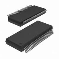
74ALVT16827DL,518 NXP Semiconductors, 74ALVT16827DL,518 Datasheet - Page 8

74ALVT16827DL,518
Manufacturer Part Number
74ALVT16827DL,518
Description
IC BUFF DVR TRI-ST 20BIT 56SSOP
Manufacturer
NXP Semiconductors
Series
74ALVTr
Datasheet
1.74ALVT16827DGG118.pdf
(16 pages)
Specifications of 74ALVT16827DL,518
Logic Type
Buffer/Line Driver, Non-Inverting
Number Of Elements
2
Number Of Bits Per Element
10
Current - Output High, Low
8mA, 8mA
Voltage - Supply
3 V ~ 3.6 V
Operating Temperature
-40°C ~ 85°C
Mounting Type
Surface Mount
Package / Case
56-SSOP
Logic Family
ALVT
Number Of Channels Per Chip
20
Polarity
Non-Inverting
Supply Voltage (max)
3.6 V
Supply Voltage (min)
2.3 V
Maximum Operating Temperature
+ 85 C
Mounting Style
SMD/SMT
High Level Output Current
- 32 mA
Low Level Output Current
64 mA
Minimum Operating Temperature
- 40 C
Number Of Lines (input / Output)
20 / 20
Output Type
3-State
Propagation Delay Time
3 ns at 2.5 V, 2.3 ns at 3.3 V
Lead Free Status / RoHS Status
Lead free / RoHS Compliant
Other names
74ALVT16827DL-T
74ALVT16827DL-T
935210040518
74ALVT16827DL-T
935210040518
Philips Semiconductors
Table 7:
At recommended operating conditions; voltages are referred to GND (ground = 0 V). T
[1]
[2]
[3]
[4]
[5]
[6]
[7]
9397 750 15122
Product data sheet
Symbol
V
V
V
V
I
I
I
I
I
I
I
LI
OFF
HOLD
EX
PU
OZ
CC
I
CC
IK
OH
OL
CC
, I
All typical values are at V
Unused pins at V
This is the bus hold overdrive current required to force the input to the opposite logic state.
This parameter is valid for any V
a transition time of 100 s is permitted. This parameter is valid for T
I
This is the increase in supply current for each input at the specified voltage level other than V
All typical values are at V
= 2.5 V
CC
PD
is measured with outputs pulled up to V
Static characteristics
Parameter
input clamp voltage
HIGH-level output
voltage
LOW-level output
voltage
input leakage current V
off current
bus hold current data
inputs
current into an
output in the
HIGH-state when
V
power-up/down
3-state output
current
3-state output
current
quiescent supply
current
additional supply
current per input pin
O
0.2 V
control pins
I/O data pins
> V
CC
CC
[7]
or GND.
CC
CC
= 3.3 V and T
= 2.5 V and T
CC
…continued
between 0 V and 1.2 V with a transition time of up to 10 ms. From V
Conditions
V
V
V
V
V
V
V
V
V
V
V
V
V
V
V
V
V
V
V
CC
CC
CC
CC
CC
CC
CC
CC
CC
CC
CC
CC
O
CC
I
CC
CC
CC
CC
CC
I
I
I
output HIGH; V
output LOW; V
outputs HIGH
outputs LOW
outputs disabled
= GND or V
OL
OL
OL
= 5.5 V; V
= 2.3 V; I
= 2.3 V to 2.7 V; I
= 2.3 V; I
= 2.3 V
= 2.3 V; I
= 2.7 V; V
= 0 V or 2.7 V; V
= 2.7 V; V
= 2.7 V; V
= 0 V; V
= 2.5 V; V
= 2.5 V; V
= 2.7 V; V
= 2.7 V; V
= 2.3 V to 2.7 V; one input at
or GND
= 100 A
= 24 mA
= 100 A
amb
amb
1.2 V; V
0.6 V, other inputs at
CC
= 25 C.
= 25 C.
or pulled down to ground.
I
CC
IK
OH
OL
or V
CC
I
I
I
I
I
I
O
O
= GND or V
= V
= V
= 0 V
= 0.8 V
= 2.0 V
= 18 mA
Rev. 03 — 2 June 2005
= 0.5 V to V
= 2.3 V
= 2.3 V; V
= 24 mA
= 8 mA
; nOEx = don’t care
O
O
O
= 0.5 V
CC
CC
= 2.3 V
= 0 V to 4.5 V
I
OH
or GND
= 5.5 V
= 100 A
I
CC
= V
CC
amb
; I
;
IL
O
= 25 C only.
or V
= 0 A
20-bit buffer/line driver; non-inverting; 3-state
IH
[2]
[2]
[2]
[3]
[3]
[4]
[5]
[6]
Min
-
V
1.8
-
-
-
-
-
-
-
-
-
-
-
-
-
-
-
-
-
-
-
CC
amb
CC
0.2 V
or GND.
© Koninklijke Philips Electronics N.V. 2005. All rights reserved.
= 40 C to +85 C .
Typ
2.1
0.07
0.3
0.07
0.3
0.1
0.1
0.1
+0.1
0.1
115
10
1
0.5
+0.5
0.04
3.6
0.04
0.04
74ALVT16827
0.85
10
CC
CC
= 1.2 V to V
Max
-
-
0.2
0.5
0.2
0.5
10
1
-
-
125
100
5
0.1
5.0
0.1
0.4
1.2
1
5
100
5
CC
= 3.3 V
Unit
V
V
V
V
V
V
V
mA
mA
mA
mA
A
A
A
A
A
A
A
A
A
A
A
8 of 16
0.3 V


