NLX2G07BMX1TCG ON Semiconductor, NLX2G07BMX1TCG Datasheet - Page 2
NLX2G07BMX1TCG
Manufacturer Part Number
NLX2G07BMX1TCG
Description
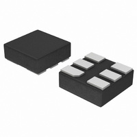
IC BUFFER DL N-INV OP/DR 6ULLGA
Manufacturer
ON Semiconductor
Datasheet
1.NLX2G07AMX1TCG.pdf
(8 pages)
Specifications of NLX2G07BMX1TCG
Logic Type
Buffer/Line Driver, Non-Inverting
Number Of Elements
2
Number Of Bits Per Element
1
Voltage - Supply
1.65 V ~ 5.5 V
Operating Temperature
-55°C ~ 125°C
Mounting Type
Surface Mount
Package / Case
6-ULLGA
Number Of Channels Per Chip
2
Polarity
Non-Inverting
Supply Voltage (max)
5.5 V
Supply Voltage (min)
1.65 V
Maximum Operating Temperature
+ 125 C
Mounting Style
Screw
Low Level Output Current
32 mA
Minimum Operating Temperature
- 55 C
Number Of Lines (input / Output)
2 / 2
Output Type
Open Drain
Propagation Delay Time
5.8 ns at 2.3 V to 2.7 V, 4.4 ns at 3 V to 3.6 V, 3.5 ns at 4.5 V to 5.5 V
Lead Free Status / RoHS Status
Lead free / RoHS Compliant
Current - Output High, Low
-
Lead Free Status / Rohs Status
Details


Stresses exceeding Maximum Ratings may damage the device. Maximum Ratings are stress ratings only. Functional operation above the
Recommended Operating Conditions is not implied. Extended exposure to stresses above the Recommended Operating Conditions may affect
device reliability.
1. Measured with minimum pad spacing on an FR4 board, using 10 mm-by-1 inch, 2 ounce copper trace no air flow.
2. Tested to EIA/JESD22-A114-A.
3. Tested to EIA/UESD22-A115-A.
4. Tested to JESD22-C101-A.
5. Tested to EIA / JESD78.
RECOMMENDED OPERATING CONDITIONS
MAXIMUM RATINGS
I
Symbol
Symbol
LATCHUP
Dt/DV
V
T
V
I
MSL
V
V
GND
V
I
I
V
STG
T
F
T
OUT
I
T
OUT
OK
I
CC
CC
IK
CC
O
IN
IN
R
A
L
J
Positive DC Supply Voltage
Digital Input Voltage
Output Voltage
Operating Free-Air Temperature
Input Transition Rise or Fall Rate
DC Supply Voltage
DC Input Voltage
DC Output Voltage
DC Input Diode Current
DC Output Diode Current
DC Output Source/Sink Current
DC Supply Current Per Supply Pin
DC Ground Current per Ground Pin
Storage Temperature Range
Lead Temperature, 1 mm from Case for 10 Seconds
Junction Temperature Under Bias
Moisture Sensitivity
Flammability Rating Oxygen
Latchup Performance Above V
CC
and Below GND at 125 °C (Note 5)
Parameter
Parameter
http://onsemi.com
NLX2G07
V
V
CC
CC
2
= 3.3 V ± 0.3 V
= 5.0 V ± 0.5 V
Index: 28 to 34
V
OUT
V
IN
< GND
< GND
UL 94 V-0 @ 0.125 in
1.65
Min
-55
0
0
0
0
-0.5 to +7.0
-0.5 to +7.0
-0.5 to +7.0
-65 to +150
Level 1
Value
±100
±100
±500
-50
-50
±50
260
150
+125
Max
100
5.5
5.5
5.5
20
ns/V
Unit
Unit
mA
mA
mA
mA
mA
mA
°C
°C
°C
°C
V
V
V
V
V
V
Related parts for NLX2G07BMX1TCG
Image
Part Number
Description
Manufacturer
Datasheet
Request
R

Part Number:
Description:
ON Semiconductor [VOLTAGE REGULATOR]
Manufacturer:
ON Semiconductor
Datasheet:
Part Number:
Description:
357-036-542-201 CARDEDGE 36POS DL .156 BLK LOPRO
Manufacturer:
ON Semiconductor
Datasheet:
Part Number:
Description:
357-036-542-201 CARDEDGE 36POS DL .156 BLK LOPRO
Manufacturer:
ON Semiconductor
Datasheet:
Part Number:
Description:
357-036-542-201 CARDEDGE 36POS DL .156 BLK LOPRO
Manufacturer:
ON Semiconductor
Datasheet:
Part Number:
Description:
357-036-542-201 CARDEDGE 36POS DL .156 BLK LOPRO
Manufacturer:
ON Semiconductor
Datasheet:
Part Number:
Description:
357-036-542-201 CARDEDGE 36POS DL .156 BLK LOPRO
Manufacturer:
ON Semiconductor
Datasheet:
Part Number:
Description:
357-036-542-201 CARDEDGE 36POS DL .156 BLK LOPRO
Manufacturer:
ON Semiconductor
Datasheet:
Part Number:
Description:
357-036-542-201 CARDEDGE 36POS DL .156 BLK LOPRO
Manufacturer:
ON Semiconductor
Datasheet:
Part Number:
Description:
357-036-542-201 CARDEDGE 36POS DL .156 BLK LOPRO
Manufacturer:
ON Semiconductor
Datasheet:
Part Number:
Description:
357-036-542-201 CARDEDGE 36POS DL .156 BLK LOPRO
Manufacturer:
ON Semiconductor
Datasheet:
Part Number:
Description:
357-036-542-201 CARDEDGE 36POS DL .156 BLK LOPRO
Manufacturer:
ON Semiconductor
Datasheet:
Part Number:
Description:
Manufacturer:
ON Semiconductor
Datasheet:
Part Number:
Description:
Manufacturer:
ON Semiconductor
Datasheet:
Part Number:
Description:
Manufacturer:
ON Semiconductor
Datasheet: