GTLP16617MTDX Fairchild Semiconductor, GTLP16617MTDX Datasheet
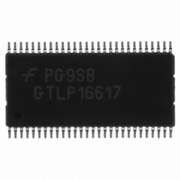
IC TRANSCVR 17BIT N-INV 56TSSOP

GTLP16617MTDX

Manufacturer Part Number
GTLP16617MTDX
Description
IC TRANSCVR 17BIT N-INV 56TSSOP
Manufacturer
Fairchild Semiconductor
Datasheet

Specifications of GTLP16617MTDX

Logic Type
Transceiver, Non-Inverting
Number Of Elements
1
Number Of Bits Per Element
17
Current - Output High, Low
32mA, 32mA
Voltage - Supply
3.15 V ~ 3.45 V
Operating Temperature
-40°C ~ 85°C
Mounting Type
Surface Mount
Package / Case
56-TSSOP
Lead Free Status / RoHS Status
Lead free / RoHS Compliant
Other names
GTLP16617MTDXTR

Available stocks

Company
Part Number
Manufacturer
Quantity
Price
Part Number:
GTLP16617MTDX
Manufacturer:
Fairchild Semiconductor
Quantity:
135
© 2000 Fairchild Semiconductor Corporation
GTLP16617MEA
GTLP16617MTD
GTLP16617
17-Bit TTL/GTLP Synchronous Bus Transceiver
with Buffered Clock
General Description
The GTLP16617 is a 17-bit registered synchronous bus
transceiver that provides TTL to GTLP signal level transla-
tion. It allows for transparent, latched and clocked modes
of data flow and provides a buffered GTLP (CLKOUT)
clock output from the TTL CLKAB. The device provides a
high speed interface between cards operating at TTL logic
levels and a backplane operating at GTLP logic levels.
High speed backplane operation is a direct result of
GTLP’s reduced output swing ( 1V), reduced input thresh-
old levels and output edge rate control. The edge rate con-
trol minimizes bus settling time. GTLP is a Fairchild
Semiconductor derivative of the Gunning Transceiver logic
(GTL) JEDEC standard JESD8-3.
Fairchild’s GTLP has internal edge-rate control and is pro-
cess, voltage, and temperature (PVT) compensated. Its
function is similar to BTL and GTL but with different output
levels and receiver threshold. GTLP output LOW level is
typically less than 0.5V, the output level HIGH is 1.5V and
the receiver threshold is 1.0V.
Ordering Code:
Devices also available in Tape and Reel. Specify by appending the suffix letter “X” to the ordering code.
Order Number
Package Number
MS56A
MTD56
56-Lead Shrink Small Outline Package (SSOP), JEDEC MO-118, 0.300 Wide
56-Lead Thin Shrink Small Outline Package (TSSOP), JEDEC MO-153, 6.1mm Wide
DS500031
Features
Bidirectional interface between GTLP and TTL logic
levels
Designed with edge rate control circuitry to reduce
output noise on the GTLP port
V
receiver threshold adjustibility
Special PVT compensation circuitry to provide
consistent performance over variations of process,
supply voltage and temperature
TTL compatible driver and control inputs
Designed using Fairchild advanced CMOS technology
Bushold data inputs on the A port eliminates the need
for external pull-up resistors on unused inputs.
Power up/down and power off high impedance for live
insertion
5 V tolerant inputs and outputs on the LVTTL port
Open drain on GTLP to support wired-or connection
Flow through pinout optimizes PCB layout
D-type flip-flop, latch and transparent data paths
A Port source/sink 32 mA/ 32 mA
GTLP Buffered CLKAB signal available (CLKOUT)
REF
Package Description
pin provides external supply reference voltage for
June 1997
Revised December 2000
www.fairchildsemi.com

Related parts for GTLP16617MTDX

GTLP16617MTDX Summary of contents

Page 1

... MTD56 56-Lead Thin Shrink Small Outline Package (TSSOP), JEDEC MO-153, 6.1mm Wide Devices also available in Tape and Reel. Specify by appending the suffix letter “X” to the ordering code. © 2000 Fairchild Semiconductor Corporation Features Bidirectional interface between GTLP and TTL logic ...

Page 2

Pin Descriptions Pin Names Description OEAB A-to-B Output Enable (Active LOW) OEBA B-to-A Output Enable (Active LOW) CEAB A-to-B Clock Enable (Active LOW) CEBA B-to-A Clock Enable (Active LOW) LEAB A-to-B Latch Enable (Transparent HIGH) LEBA B-to-A Latch Enable (Transparent ...

Page 3

Logic Diagram 3 www.fairchildsemi.com ...

Page 4

Absolute Maximum Ratings Supply Voltage ( Input Voltage ( Output Voltage ( Outputs 3-STATE Outputs Active (Note 7) 0. Output Sink Current into A Port Output ...

Page 5

DC Electrical Characteristics Symbol 3.45V, CCQ Ports V 5.25V, CCQ CCQ GND I CCQ 3.45V ...

Page 6

AC Electrical Characteristics Over recommended range of supply voltage and operating free-air temperature for B Port and for A Port Symbol From (Input PLH t PHL t LEAB PLH ...

Page 7

Test Circuits and Timing Waveforms Test Circuit for A Outputs C includes probes and jig capacitance. L Voltage Waveforms Pulse Duration (Vm Voltage Waveforms Propagation Delay and Setup and Hold Times (Vm Voltage Waveforms Enable and Disable Times (A Port) ...

Page 8

Physical Dimensions inches (millimeters) unless otherwise noted 56-Lead Shrink Small Outline Package (SSOP), JEDEC MO-118, 0.300 Wide www.fairchildsemi.com Package Number MS56A 8 ...

Page 9

Physical Dimensions inches (millimeters) unless otherwise noted (Continued) 56-Lead Thin Shrink Small Outline Package (TSSOP), JEDEC MO-153, 6.1mm Wide Fairchild does not assume any responsibility for use of any circuitry described, no circuit patent licenses are implied and Fairchild reserves ...

Related keywords