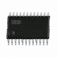
74ABT651PW,112 NXP Semiconductors, 74ABT651PW,112 Datasheet - Page 2

74ABT651PW,112
Manufacturer Part Number
74ABT651PW,112
Description
IC TRANSCVR 3ST 8BIT INV 24TSSOP
Manufacturer
NXP Semiconductors
Series
74ABTr
Datasheet
1.74ABT651PW112.pdf
(13 pages)
Specifications of 74ABT651PW,112
Logic Type
Transceiver, Non-Inverting
Number Of Elements
1
Number Of Bits Per Element
8
Current - Output High, Low
32mA, 64mA
Voltage - Supply
4.5 V ~ 5.5 V
Operating Temperature
-40°C ~ 85°C
Mounting Type
Surface Mount
Package / Case
24-TSSOP
Lead Free Status / RoHS Status
Lead free / RoHS Compliant
Other names
568-2490-5
935178880112
935178880112
Philips Semiconductors
FEATURES
QUICK REFERENCE DATA
ORDERING INFORMATION
PIN CONFIGURATION
24-Pin Plastic DIP
24-Pin plastic SO
24-Pin Plastic TSSOP Type I
2002 Dec 17
Independent registers for A and B buses
The 74ABT651 is the inverting version of the 74ABT652
Multiplexed real-time and stored data
3-State outputs
Live insertion/extraction permitted.
Power-up 3-State
Power-up reset
Output capability: +64 mA / –32 mA
Latch-up protection exceeds 500 mA per Jedec Std 17
ESD protection exceeds 2000 V per MIL STD 883 Method 3015
and 200 V per Machine Model
Octal transceiver/register, inverting (3-State)
SYMBOL
t
t
I
C
C
CCZ
PLH
PHL
I/O
IN
PACKAGES
OEAB
CPAB
GND
SAB
Propagation delay
CPBA to An or CPAB to Bn
Input capacitance
I/O capacitance
Total supply current
A0
A1
A2
A3
A4
A5
A6
A7
10
12
11
1
2
3
4
5
6
7
8
9
PARAMETER
SA00094
24
23
22
21
20
19
18
17
16
15
14
13
V
CPBA
SBA
OEBA
B0
B1
B2
B3
B4
B5
B6
B7
CC
TEMPERATURE RANGE
–40 C to +85 C
–40 C to +85 C
–40 C to +85 C
C
V
Outputs disabled; V
Outputs disabled; V
I
L
= 0 V or V
= 50 pF; V
2
DESCRIPTION
The 74ABT651 high-performance BiCMOS device combines low
static and dynamic power dissipation with high speed and high
output drive.
The 74ABT651 transceiver/register consists of bus transceiver
circuits with 3-State outputs, D-type flip-flops, and control circuitry
arranged for multiplexed transmission of data directly from the input
bus or the internal registers. Data on the A or B bus will be clocked
into the registers as the appropriate clock pin goes HIGH. Output
Enable (OEAB, OEBA) and Select (SAB, SBA) pins are provided for
bus management.
The following examples demonstrate the four fundamental
bus-management functions that can be performed with the
74ABT651.
The select pins determine whether data is stored or transferred
through the device in real time.
The output enable pins determine the direction of the data flow.
PIN DESCRIPTION
4, 5, 6, 7, 8,
T
20, 19, 18,
17, 16, 15,
NUMBER
amb
9, 10, 11
14, 13
CC
1, 23
2, 22
3, 21
PIN
CC
12
24
CONDITIONS
= 25 C; GND = 0 V
= 5 V
O
CC
= 0 V or V
= 5.5 V
PART NUMBER
SYMBOL
A0 – A7
B0 – B7
74ABT651PW
OEAB /
CPAB /
OEBA
74ABT651N
74ABT651D
CPBA
SAB /
GND
SBA
V
CC
CC
A to B clock input /
B to A clock input
A to B select input /
B to A select input
A to B Output Enable input /
B to A Output Enable input
(active–LOW)
Data inputs/outputs (A side)
Data inputs/outputs (B side)
Ground (0 V)
Positive supply voltage
FUNCTION
TYPICAL
110
3.8
4.4
74ABT651
4
7
DWG NUMBER
SOT222-1
SOT137-1
SOT355-1
Product data
UNIT
pF
pF
ns
A


