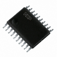
74ABT2241PW,118 NXP Semiconductors, 74ABT2241PW,118 Datasheet - Page 2

74ABT2241PW,118
Manufacturer Part Number
74ABT2241PW,118
Description
IC BUFF/DVR TRI-ST DUAL 20TSSOP
Manufacturer
NXP Semiconductors
Series
74ABTr
Datasheet
1.74ABT2241D112.pdf
(12 pages)
Specifications of 74ABT2241PW,118
Logic Type
Buffer/Line Driver, Non-Inverting
Number Of Elements
2
Number Of Bits Per Element
4
Current - Output High, Low
32mA, 12mA
Voltage - Supply
4.5 V ~ 5.5 V
Operating Temperature
-40°C ~ 85°C
Mounting Type
Surface Mount
Package / Case
20-TSSOP
Lead Free Status / RoHS Status
Lead free / RoHS Compliant
Other names
74ABT2241PW-T
74ABT2241PW-T
935220720118
74ABT2241PW-T
935220720118
Philips Semiconductors
FEATURES
QUICK REFERENCE DATA
ORDERING INFORMATION
PIN CONFIGURATION
20-Pin Plastic DIP
20-Pin plastic SO
20-Pin Plastic SSOP Type II
20-Pin Plastic TSSOP Type I
1996 Sep 30
Octal bus interface
3-State buffers
Power-up 3-State
Output capability: +12mA/–32mA
Latch-up protection exceeds 500mA per Jedec Std 17
ESD protection exceeds 2000 V per MIL STD 883 Method 3015
and 200 V per Machine Model
Octal buffer with 30W series termination resistors
(3-State)
SYMBOL
C
I
t
t
C
PLH
PHL
CCZ
OUT
IN
PACKAGES
GND
1OE
1A0
2Y0
1A1
2Y1
1A2
2Y2
1A3
2Y3
Propagation delay
An to Yn
Input capacitance
Output capacitance
Total supply current
10
1
2
3
4
5
6
7
8
9
PARAMETER
TEMPERATURE RANGE
20
19
18
17
16
15
14
13
12
11
V
2OE
1Y0
2A0
1Y1
2A1
1Y2
2A2
1Y3
2A3
–40 C to +85 C
–40 C to +85 C
–40 C to +85 C
–40 C to +85 C
CC
C
V
Outputs disabled; V
Outputs disabled; V
SA00038
I
L
= 0V or V
= 50pF; V
OUTSIDE NORTH AMERICA
2
CC
T
CC
amb
74ABT2241 PW
74ABT2241 DB
DESCRIPTION
The 74ABT2241 high-performance BiCMOS device combines low
static and dynamic power dissipation with high speed and high
output drive.
The 74ABT2241 device is an octal buffer that is ideal for driving bus
lines. The device features two Output Enables (1OE, 2OE), each
controlling four of the 3-State outputs.
The 74ABT2241 is designed with 30W series resistance in both the
High and Low states of the output. The design reduces line noise in
applications such as memory address drivers, clock drivers, and bus
receivers/transceivers.
PIN DESCRIPTION
= 5V
74ABT2241 N
74ABT2241 D
PIN NUMBER
CONDITIONS
17, 15, 13, 11
18, 16, 14, 12
= 25 C; GND = 0V
O
CC
2, 4, 6, 8
3, 5, 7, 9
= 0V or V
1, 19
= 5.5V
10
20
CC
1A0 – 1A3
2A0 – 2A3
1Y0 – 1Y3
2Y0 – 2Y3
1OE, 2OE
SYMBOL
GND
V
CC
NORTH AMERICA
7ABT2241PW DH
74ABT2241 DB
74ABT2241 N
74ABT2241 D
Data inputs
Data inputs
Data outputs
Data outputs
Output enables
Ground (0V)
Positive supply voltage
NAME AND FUNCTION
TYPICAL
2.9
50
3
7
74ABT2241
Product specification
DWG NUMBER
853–1879 17325
SOT146-1
SOT163-1
SOT339-1
SOT360-1
UNIT
pF
pF
ns
A


