MC74VHCT126ADR2G ON Semiconductor, MC74VHCT126ADR2G Datasheet
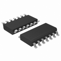
IC BUS BUFF TRI-ST QUAD 14SOIC

MC74VHCT126ADR2G

Manufacturer Part Number
MC74VHCT126ADR2G
Description
IC BUS BUFF TRI-ST QUAD 14SOIC
Manufacturer
ON Semiconductor
Series
74VHCTr
Datasheet

Specifications of MC74VHCT126ADR2G

Logic Type
Buffer/Line Driver, Non-Inverting
Number Of Elements
4
Number Of Bits Per Element
1
Current - Output High, Low
8mA, 8mA
Voltage - Supply
4.5 V ~ 5.5 V
Operating Temperature
-40°C ~ 85°C
Mounting Type
Surface Mount
Package / Case
14-SOIC (3.9mm Width), 14-SOL
Logic Family
VHCT
Number Of Channels Per Chip
4
Polarity
Non-Inverting
Supply Voltage (max)
5.5 V
Supply Voltage (min)
4.5 V
Maximum Operating Temperature
+ 85 C
Mounting Style
SMD/SMT
High Level Output Current
- 8 mA
Low Level Output Current
8 mA
Maximum Power Dissipation
500 mW
Minimum Operating Temperature
- 40 C
Number Of Lines (input / Output)
4 / 3
Output Type
3-State
Propagation Delay Time
11.5 ns at 3.3 V, 7.5 ns at 5 V
Lead Free Status / RoHS Status
Lead free / RoHS Compliant

Available stocks

Company
Part Number
Manufacturer
Quantity
Price
Part Number:
MC74VHCT126ADR2G
Manufacturer:
ON Semiconductor
Quantity:
8
MC74VHCT126A
Quad Bus Buffer
with 3−State Control Inputs
fabricated with silicon gate CMOS technology. It achieves
noninverting high speed operation similar to equivalent Bipolar
Schottky TTL while maintaining CMOS low power dissipation.
set Low to place the output into high impedance.
be used as a level converter for interfacing 3.3 V to 5.0 V, because it
has full 5.0 V CMOS level output swings.
between 0 V and 5.5 V are applied, regardless of the supply voltage.
The output structures also provide protection when V
input and output structures help prevent device destruction caused by
supply voltage − input/output voltage mismatch, battery backup, hot
insertion, etc.
output which provides high noise immunity and stable output. The
inputs tolerate voltages up to 7.0 V, allowing the interface of 5.0 V
systems to 3.0 V systems.
Features
*For additional information on our Pb−Free strategy and soldering details, please
© Semiconductor Components Industries, LLC, 2008
October, 2008 − Rev. 6
download the ON Semiconductor Soldering and Mounting Techniques
Reference Manual, SOLDERRM/D.
The MC74VHCT126A is a high speed CMOS quad bus buffer
The MC74VHCT126A requires the 3−state control input (OE) to be
The VHCT inputs are compatible with TTL levels. This device can
The VHCT126A input structures provide protection when voltages
The internal circuit is composed of three stages, including a buffer
High Speed: t
Low Power Dissipation: I
TTL−Compatible Inputs: V
Power Down Protection Provided on Inputs
Balanced Propagation Delays
Designed for 2.0 V to 5.5 V Operating Range
Low Noise: V
Pin and Function Compatible with Other Standard Logic Families
Latchup Performance Exceeds 300 mA
ESD Performance: HBM > 2000 V; Machine Model > 200 V
Chip Complexity: 72 FETs or 18 Equivalent Gates
Pb−Free Packages are Available*
PD
OLP
= 3.8 ns (Typ) at V
= 0.8 V (Max)
CC
IL
= 4.0 mA (Max) at T
= 0.8 V; V
CC
= 5.0 V
IH
= 2.0 V
A
CC
= 25°C
= 0 V. These
1
See detailed ordering and shipping information in the package
dimensions section on page 4 of this data sheet.
1
A
H
X
1
L
1
Inputs
See Applications Note #AND8004/D for
ORDERING INFORMATION
A
WL, L
Y
WW, W = Work Week
G or G
date code and traceability information.
http://onsemi.com
FUNCTION TABLE
CASE 948G
OE
DT SUFFIX
CASE 751A
TSSOP−14
SOEIAJ−14
H
H
L
M SUFFIX
CASE 965
D SUFFIX
SOIC−14
= Assembly Location
= Wafer Lot
= Year
= Pb−Free Package
VHCT126A
Publication Order Number:
14
14
1
MC74VHCT126A/D
1
14
Outputs
1
DIAGRAMS
VHCT126AG
MARKING
AWLYWW
VHCT126
ALYWG
Y
H
L
Z
ALYWG
VHCT
126A
G

Related parts for MC74VHCT126ADR2G

MC74VHCT126ADR2G Summary of contents

Page 1

... Chip Complexity: 72 FETs or 18 Equivalent Gates • Pb−Free Packages are Available* *For additional information on our Pb−Free strategy and soldering details, please download the ON Semiconductor Soldering and Mounting Techniques Reference Manual, SOLDERRM/D. © Semiconductor Components Industries, LLC, 2008 October, 2008 − Rev ...

Page 2

A1 1 OE1 OE2 OE3 OE4 Figure 1. LOGIC DIAGRAM Active−High Output Enables Î Î Î Î Î Î Î Î Î Î Î Î Î Î Î Î Î ...

Page 3

DC ELECTRICAL CHARACTERISTICS Î Î Î Î ...

Page 4

... UNDER TEST *Includes all probe and jig capacitance Figure 5. Test Circuit ORDERING INFORMATION Device MC74VHCT126ADR2 MC74VHCT126ADR2G MC74VHCT126AM MC74VHCT126AMG MC74VHCT126AMEL MC74VHCT126AMELG MC74VHCT126ADTRG †For information on tape and reel specifications, including part orientation and tape sizes, please refer to our Tape and Reel Packaging Specifications Brochure, BRD8011/D. ...

Page 5

G −T− SEATING 14 PL PLANE 0.25 (0.010 14X REF 0.10 (0.004) 0.15 (0.006 L PIN 1 IDENT. 1 0.15 (0.006) T ...

Page 6

... Opportunity/Affirmative Action Employer. This literature is subject to all applicable copyright laws and is not for resale in any manner. PUBLICATION ORDERING INFORMATION LITERATURE FULFILLMENT: Literature Distribution Center for ON Semiconductor P.O. Box 5163, Denver, Colorado 80217 USA Phone: 303−675−2175 or 800−344−3860 Toll Free USA/Canada Fax: 303− ...

Related keywords