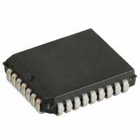
CY7C421-20JXC Cypress Semiconductor Corp, CY7C421-20JXC Datasheet - Page 3

CY7C421-20JXC
Manufacturer Part Number
CY7C421-20JXC
Description
IC ASYNC FIFO MEM 512X9 32-PLCC
Manufacturer
Cypress Semiconductor Corp
Series
CY7Cr
Specifications of CY7C421-20JXC
Access Time
10ns
Memory Size
4.6K (512 x 9)
Package / Case
32-PLCC
Function
Asynchronous
Data Rate
50MHz
Voltage - Supply
3.3V
Operating Temperature
-40°C ~ 85°C
Mounting Type
Surface Mount
Number Of Circuits
2
Data Bus Width
9 bit
Bus Direction
Unidirectional
Timing Type
Asynchronous
Organization
512 K x 9
Supply Voltage (max)
5.5 V
Supply Voltage (min)
4.5 V
Maximum Operating Current
55 mA
Maximum Operating Temperature
+ 70 C
Minimum Operating Temperature
0 C
Mounting Style
SMD/SMT
Configuration
Dual
Density
4.5Kb
Access Time (max)
20ns
Word Size
9b
Sync/async
Asynchronous
Expandable
Yes
Package Type
PLCC
Clock Freq (max)
Not RequiredMHz
Operating Supply Voltage (typ)
5V
Operating Supply Voltage (min)
4.5V
Operating Supply Voltage (max)
5.5V
Supply Current
55mA
Operating Temp Range
0C to 70C
Operating Temperature Classification
Commercial
Mounting
Surface Mount
Pin Count
32
Rohs Compliant
YES
Lead Free Status / RoHS Status
Lead free / RoHS Compliant
Lead Free Status / RoHS Status
Lead free / RoHS Compliant, Lead free / RoHS Compliant
Other names
428-2911-5
CY7C421-20JXC
CY7C421-20JXC
Available stocks
Company
Part Number
Manufacturer
Quantity
Price
Company:
Part Number:
CY7C421-20JXC
Manufacturer:
Cypress Semiconductor Corp
Quantity:
10 000
Part Number:
CY7C421-20JXC
Manufacturer:
CYPRESS/赛普拉斯
Quantity:
20 000
Company:
Part Number:
CY7C421-20JXCT
Manufacturer:
Cypress Semiconductor Corp
Quantity:
10 000
Maximum Rating
Exceeding maximum ratings may impair the useful life of the
device. These user guidelines are not tested.
Storage Temperature ................................. –65
Ambient Temperature with Power Applied.. –55
Supply Voltage to Ground Potential................–0.5V to +7.0V
DC Voltage Applied to Outputs
in High Z State ................................................–0.5V to +7.0V
DC Input Voltage ............................................–0.5V to +7.0V
Power Dissipation.......................................................... 1.0W
Electrical Characteristics
Document #: 38-06001 Rev. *C
Notes
V
V
V
V
I
I
I
Parameter
1. Single Power Supply: The voltage on any input or I/O pin can not exceed the power pin during power-up.
2. T
3. See the last page of this specification for Group A subgroup testing information.
4. V
5. For test purposes, not more than one output at a time should be shorted. Short circuit test duration should not exceed 30 seconds.
IX
OZ
OS
OH
OL
IH
IL
A
IL
is the “instant on” case temperature.
(Min.) = –2.0V for pulse durations of less than 20 ns.
Output HIGH Voltage
Output LOW Voltage
Input HIGH Voltage
Input LOW Voltage
Input Leakage Current
Output Leakage Current
Output Short Circuit Current
Description
Over the Operating Range
[5]
[1]
°
°
C to +150
C to +125
V
V
GND < V
R > V
V
CC
CC
CC
= Min., I
= Min., I
= Max., V
IH
, GND < V
I
°
°
Test Conditions
C
C
< V
OH
OL
CC
OUT
[3]
= 8.0 mA
= –2.0 mA
O
= GND
Output Current, into Outputs (LOW)............................ 20 mA
Static Discharge Voltage............................................ >2000V
(per MIL–STD–883, Method 3015)
Latch-Up Current ..................................................... >200 mA
Operating Range
< V
Commercial
Industrial
Commercial
Industrial
CC
Range
Ambient Temperature
–40
0
°
Min
–10
–10
2.4
2.0
2.2
C to + 70
[4]
°
C to +85
CY7C419/21/25/29/33
All Speed Grades
°
C
°
C
[2]
Max
V
V
+10
+10
–90
0.4
0.8
CC
CC
5V ± 10%
5V ± 10%
Page 3 of 17
V
CC
Unit
mA
μA
μA
V
V
V
V
[+] Feedback


