CY7C4241V-15AXC Cypress Semiconductor Corp, CY7C4241V-15AXC Datasheet - Page 3
CY7C4241V-15AXC
Manufacturer Part Number
CY7C4241V-15AXC
Description
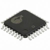
IC SYNC FIFO MEM 4KX9 32-TQFP
Manufacturer
Cypress Semiconductor Corp
Series
CY7Cr
Specifications of CY7C4241V-15AXC
Function
Synchronous
Memory Size
36K (4K x 9)
Data Rate
100MHz
Access Time
10ns
Voltage - Supply
3.3V
Operating Temperature
-40°C ~ 85°C
Mounting Type
Surface Mount
Package / Case
32-TQFP
Configuration
Dual
Density
36Kb
Access Time (max)
11ns
Word Size
9b
Organization
4Kx9
Sync/async
Synchronous
Expandable
Yes
Bus Direction
Uni-Directional
Package Type
TQFP
Clock Freq (max)
66.7MHz
Operating Supply Voltage (typ)
3.3V
Operating Supply Voltage (min)
3V
Operating Supply Voltage (max)
3.6V
Supply Current
20mA
Operating Temp Range
0C to 70C
Operating Temperature Classification
Commercial
Mounting
Surface Mount
Pin Count
32
Lead Free Status / RoHS Status
Lead free / RoHS Compliant
Available stocks
Company
Part Number
Manufacturer
Quantity
Price
Company:

Part Number:
CY7C4241V-15AXC
Manufacturer:
CY
Quantity:
21
Company:
Part Number:
CY7C4241V-15AXC
Manufacturer:
Cypress Semiconductor Corp
Quantity:
10 000
Company:
Part Number:
CY7C4241V-15AXCT
Manufacturer:
Cypress Semiconductor Corp
Quantity:
10 000


Pin Configuration
Figure 1. 32-Pin PLCC
Selection Guide
Pin Definitions
Document #: 38-06010 Rev. *C
Maximum Frequency
Maximum Access Time
Minimum Cycle Time
Minimum Data or Enable Set-up
Minimum Data or Enable Hold
Maximum Flag Delay
Active Power Supply Current
D
Q
WEN1
WEN2/LD
Dual Mode Pin
REN1, REN2
WCLK
Signal Name
Density
0−8
0−8
CY7C4421V
REN1
RCLK
REN2
Data Inputs
Data Outputs
Write Enable 1
Write Enable 2
Load
Read Enable
Inputs
Write Clock
GND
PAE
PAF
64 x 9
OE
D
D
Description
Description
1
0
5
6
7
8
9
10
11
12
13
14151617 181920
4 3 2 1
Top View
CY7C4201V
32
3130
256 x 9
I/O
29
28
27
26
25
24
23
22
21
Commercial
O Data Outputs for 9-bit bus.
I
I
I
I
I
I
RS
WEN1
WCLK
WEN2/LD
V
Q
Q
Q
Q
Data Inputs for 9-bit bus.
The only write enable when device is configured to have programmable flags.
Data is written on a LOW-to-HIGH transition of WCLK when WEN1 is asserted and FF is
HIGH. If the FIFO is configured to have two write enables, data is written on a LOW-to-HIGH
transition of WCLK when WEN1 is LOW and WEN2/LD and FF are HIGH.
If HIGH at reset, this pin operates as a second write enable. If LOW at reset, this
pin operates as a control to write or read the programmable flag offsets. WEN1 must be
LOW and WEN2 must be HIGH to write data into the FIFO. Data will not be written into the FIFO
if the FF is LOW. If the FIFO is configured to have programmable flags, WEN2/LD is held LOW
to write or read the programmable flag offsets.
Enables the device for Read operation.
The rising edge clocks data into the FIFO when WEN1 is LOW and WEN2/LD is HIGH
and the FIFO is not Full. When LD is asserted, WCLK writes data into the programmable
flag-offset register.
CC
8
7
6
5
CY7C4211V
512 x 9
CY7C42X1V-15
66.7
11
15
10
20
4
1
CY7C4221V
1K x 9
Figure 2. 32-Pin TQFP
CY7C42X1V-25
Description
CY7C4231V
2K x 9
40
15
25
15
20
6
1
CY7C4201V/4211V/4221V
CY7C4241V
4K x 9
CY7C42X1V-35
CY7C4241V/4251V
28.6
20
35
20
20
7
2
CY7C4251V
8K x 9
Page 3 of 19
MHz
Unit
mA
ns
ns
ns
ns
ns
[+] Feedback
Related parts for CY7C4241V-15AXC
Image
Part Number
Description
Manufacturer
Datasheet
Request
R

Part Number:
Description:
IC SYNC FIFO MEM 4KX9 32-PLCC
Manufacturer:
Cypress Semiconductor Corp
Datasheet:
Part Number:
Description:
IC SYNC FIFO MEM 4KX9 32-PLCC
Manufacturer:
Cypress Semiconductor Corp
Datasheet:

Part Number:
Description:
Manufacturer:
Cypress Semiconductor Corp
Datasheet:
Part Number:
Description:
Manufacturer:
Cypress Semiconductor Corp
Datasheet:

Part Number:
Description:
IC SYNC FIFO MEM 4KX9 32-TQFP
Manufacturer:
Cypress Semiconductor Corp
Datasheet:
Part Number:
Description:
IC SYNC FIFO MEM 4KX9 32-PLCC
Manufacturer:
Cypress Semiconductor Corp
Datasheet:
Part Number:
Description:
IC SYNC FIFO MEM 4KX9 32-TQFP
Manufacturer:
Cypress Semiconductor Corp
Datasheet:
Part Number:
Description:
IC SYNC FIFO MEM 4KX9 32-TQFP
Manufacturer:
Cypress Semiconductor Corp
Datasheet:
Part Number:
Description:
IC SYNC FIFO MEM 4KX9 32-PLCC
Manufacturer:
Cypress Semiconductor Corp
Datasheet:
Part Number:
Description:
Manufacturer:
Cypress Semiconductor Corp
Datasheet:

Part Number:
Description:
Manufacturer:
Cypress Semiconductor Corp
Datasheet:
Part Number:
Description:
Manufacturer:
Cypress Semiconductor Corp
Datasheet:
Part Number:
Description:
Manufacturer:
Cypress Semiconductor Corp
Datasheet:
Part Number:
Description:
IC SYNC FIFO MEM 4KX9 32-PLCC
Manufacturer:
Cypress Semiconductor Corp
Datasheet:
Part Number:
Description:
IC SYNC FIFO MEM 4KX9 32-TQFP
Manufacturer:
Cypress Semiconductor Corp
Datasheet: