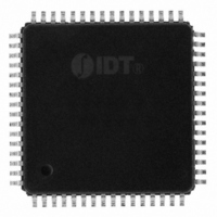
IDT72V271LA10PFG IDT, Integrated Device Technology Inc, IDT72V271LA10PFG Datasheet - Page 17

IDT72V271LA10PFG
Manufacturer Part Number
IDT72V271LA10PFG
Description
IC FIFO SYNC 3.3V 10NS 64-TQFP
Manufacturer
IDT, Integrated Device Technology Inc
Series
72Vr
Datasheet
1.IDT72V271LA10PFG.pdf
(27 pages)
Specifications of IDT72V271LA10PFG
Function
Synchronous
Memory Size
288K (16K x 18)
Access Time
10ns
Voltage - Supply
3 V ~ 3.6 V
Operating Temperature
0°C ~ 70°C
Mounting Type
Surface Mount
Package / Case
64-TQFP, 64-VQFP
Configuration
Dual
Density
288Kb
Access Time (max)
6.5ns
Word Size
9b
Organization
32Kx9
Sync/async
Synchronous
Expandable
Yes
Bus Direction
Uni-Directional
Package Type
TQFP
Clock Freq (max)
100MHz
Operating Supply Voltage (typ)
3.3V
Operating Supply Voltage (min)
3V
Operating Supply Voltage (max)
3.6V
Supply Current
55mA
Operating Temp Range
0C to 70C
Operating Temperature Classification
Commercial
Mounting
Surface Mount
Pin Count
64
Lead Free Status / RoHS Status
Lead free / RoHS Compliant
Data Rate
-
Lead Free Status / Rohs Status
Compliant
Other names
72V271LA10PFG
800-1523
800-1523
Available stocks
Company
Part Number
Manufacturer
Quantity
Price
Company:
Part Number:
IDT72V271LA10PFG
Manufacturer:
IDT, Integrated Device Technology Inc
Quantity:
10 000
Company:
Part Number:
IDT72V271LA10PFG8
Manufacturer:
IDT, Integrated Device Technology Inc
Quantity:
10 000
NOTES:
1. t
2. LD = HIGH.
3. First word latency: 60ns + t
NOTES:
1. t
2. LD = HIGH, OE = LOW, EF = HIGH
IDT72V261LA/72V271LA
3.3 VOLT CMOS SuperSync FIFO™ 16,384 x 9 and 32,768 x 9
Q
D
Q
D
WCLK
edge of WCLK and the rising edge of RCLK is less than t
WCLK
RCLK
0
0
rising edge of the RCLK and the rising edge of the WCLK is less than t
0
0
SKEW3
RCLK
SKEW1
WEN
WEN
REN
REN
- Q
- D
- D
- Q
OE
EF
FF
n
n
n
n
is the minimum time between a rising WCLK edge and a rising RCLK edge to guarantee that EF will go HIGH (after one RCLK cycle plus t
is the minimum time between a rising RCLK edge and a rising WCLK edge to guarantee that FF will go high (after one WCLK cycle pus t
t
ENS
t
DATA IN OUTPUT REGISTER
ENS
t
t
SKEW1
OLZ
t
ENH
t
Figure 8. Read Cycle, Empty Flag and First Data Word Latency Timing (IDT Standard Mode)
REF
REF
t
A
t
OE
(1)
+ 1*T
t
t
RCLK
SKEW3
ENH
t
ENS
t
t
DS
A
.
D
(1)
1
0
NO WRITE
Figure 7. Write Cycle and Full Flag Timing (IDT Standard Mode)
NO OPERATION
t
t
DHS
ENH
LAST WORD
1
SKEW3
2
, then EF deassertion may be delayed one extra RCLK cycle.
t
WFF
t
t
SKEW1
DS
OHZ
t
t
DS
t
ENS
CLKH
, then the FF deassertion may be delayed one extra WCLK cycle.
D
D
1
X
NO OPERATION
t
WFF
t
t
ENH
DATA READ
DH
17
t
DH
t
CLK
2
t
CLKL
t
CLKH
t
t
ENS
REF
t
OLZ
t
SKEW1
t
CLK
(1)
t
CLKL
t
ENS
t
ENH
LAST WORD
t
A
1
NO WRITE
COMMERCIAL AND INDUSTRIAL
t
ENH
t
A
TEMPERATURE RANGES
2
REF
WFF
). If the time between the rising
NEXT DATA READ
). If the time between the
t
t
ENS
WFF
t
DS
JANUARY 30, 2009
D
0
D
X
+1
t
REF
t
t
ENH
A
4673 drw10
t
DH
t
WFF
4673 drw 11
D
1


