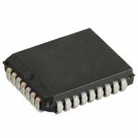
CY7C4241V-15JC Cypress Semiconductor Corp, CY7C4241V-15JC Datasheet - Page 4

CY7C4241V-15JC
Manufacturer Part Number
CY7C4241V-15JC
Description
IC SYNC FIFO MEM 4KX9 32-PLCC
Manufacturer
Cypress Semiconductor Corp
Series
CY7Cr
Datasheet
1.CY7C4201V-15AC.pdf
(17 pages)
Specifications of CY7C4241V-15JC
Function
Synchronous
Memory Size
36K (4K x 9)
Data Rate
100MHz
Access Time
10ns
Voltage - Supply
3.3V
Operating Temperature
-40°C ~ 85°C
Mounting Type
Surface Mount
Package / Case
32-PLCC
Lead Free Status / RoHS Status
Contains lead / RoHS non-compliant
Other names
428-1224
Available stocks
Company
Part Number
Manufacturer
Quantity
Price
Company:
Part Number:
CY7C4241V-15JC
Manufacturer:
CY
Quantity:
92
Company:
Part Number:
CY7C4241V-15JC
Manufacturer:
Cypress Semiconductor Corp
Quantity:
10 000
Document #: 38-06010 Rev. *A
Programmable Flag (PAE, PAF) Operation
Whether the flag offset registers are programmed as described
in Table 1 or the default values are used, the programmable
Almost Empty Flag (PAE) and programmable Almost Full Flag
(PAF) states are determined by their corresponding offset
registers and the difference between the read and write
pointers.
Table 1. Writing the Offset Registers
Note:
1.
LD
0
0
1
1
8
8
8
8
The same selection sequence applies to reading from the registers. REN1 and REN2 are enabled and a read is performed on the LOW-to-HIGH transition of RCLK.
WEN
64 x 9
0
1
0
1
6
6
Empty Offset (LSB) Reg.
Default Value = 007h
Full Offset (LSB) Reg
Default Value = 007h
WCLK
8
8
8
8
[1]
Empty Offset (LSB) Reg.
Default Value = 007h
Full Offset (LSB) Reg
Default Value = 007h
7
7
2K x 9
0
0
0
0
Empty Offset (LSB)
Empty Offset (MSB)
Full Offset (LSB)
Full Offset (MSB)
No Operation
Write Into FIFO
No Operation
2
2
(MSB)
(MSB)
000
000
8
8
8
8
Figure 1. Offset Register Location and Default Values
256 x 9
Selection
Empty Offset (LSB) Reg.
Default Value = 007h
7
7
Full Offset (LSB) Reg
Default Value = 007h
0
0
0
0
8
8
8
8
Empty Offset (LSB) Reg.
Default Value = 007h
Full Offset (LSB) Reg
Default Value = 007h
7
7
0
0
0
0
4K x 9
3
3
(MSB)
(MSB)
0000
0000
8
8
8
8
The number formed by the empty offset least significant bit
register and empty offset most significant register is referred
to as n and determines the operation of PAE. PAE is synchro-
nized to the LOW-to-HIGH transition of RCLK by one flip-flop
and is LOW when the FIFO contains n or fewer unread words.
PAE is set HIGH by the LOW-to-HIGH transition of RCLK
when the FIFO contains (n+1) or greater unread words.
The number formed by the full offset least significant bit
register and full offset most significant bit register is referred to
as m and determines the operation of PAF. PAE is synchro-
nized to the LOW-to-HIGH transition of WCLK by one flip-flop
and is set LOW when the number of unread words in the FIFO
is greater than or equal to CY7C4421V (64 – m), CY7C4201V
(256 – m), CY7C4211V (512 – m), CY7C4221V (1K – m),
CY7C4231V (2K – m), CY7C4241V (4K – m), and
CY7C4251V (8K – m). PAF is set HIGH by the LOW-to-HIGH
transition of WCLK when the number of available memory
locations is greater than m.
512 x 9
Empty Offset (LSB) Reg.
Default Value = 007h
Full Offset (LSB) Reg
Default Value = 007h
7
7
0
0
0
0
CY7C4421V/4201V/4211V/4221V
8
8
8
8
(MSB)
CY7C4231V/4241V/4251V
(MSB)
0
0
0
0
0
0
Empty Offset (LSB) Reg.
Default Value = 007h
Full Offset (LSB) Reg
Default Value = 007h
7
7
8K x 9
4
4
8
8
8
8
(MSB)
00000
(MSB)
00000
Empty Offset (LSB) Reg.
Default Value = 007h
Full Offset (LSB) Reg
Default Value = 007h
1K x 9
7
7
0
0
0
0
1
1
(MSB)
(MSB)
00
00
Page 4 of 17
0
0
0
0


