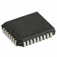
CY7C4291-10JC Cypress Semiconductor Corp, CY7C4291-10JC Datasheet - Page 12

CY7C4291-10JC
Manufacturer Part Number
CY7C4291-10JC
Description
IC DEEP SYNC FIFO 128KX9 32-PLCC
Manufacturer
Cypress Semiconductor Corp
Series
CY7Cr
Datasheet
1.CY7C4291-10JC.pdf
(16 pages)
Specifications of CY7C4291-10JC
Function
Synchronous
Memory Size
1.1M (128K x 9)
Data Rate
100MHz
Access Time
8ns
Voltage - Supply
3.3V
Operating Temperature
-40°C ~ 85°C
Mounting Type
Surface Mount
Package / Case
32-PLCC
Configuration
Dual
Density
1.125Mb
Access Time (max)
8ns
Word Size
9b
Organization
128Kx9
Sync/async
Synchronous
Expandable
Yes
Bus Direction
Uni-Directional
Package Type
PLCC
Clock Freq (max)
100MHz
Operating Supply Voltage (typ)
5V
Operating Supply Voltage (min)
4.5V
Operating Supply Voltage (max)
5.5V
Supply Current
40mA
Operating Temp Range
0C to 70C
Operating Temperature Classification
Commercial
Mounting
Surface Mount
Pin Count
32
Lead Free Status / RoHS Status
Contains lead / RoHS non-compliant
Other names
428-1244
Available stocks
Company
Part Number
Manufacturer
Quantity
Price
Company:
Part Number:
CY7C4291-10JC
Manufacturer:
Cypress Semiconductor Corp
Quantity:
10 000
Document #: 38-06007 Rev. *B
Switching Waveforms
Notes:
20. t
21. PAE offset = n.
22. If a read is preformed on this rising edge of the read clock, there will be Empty + (n 1) words in the FIFO when PAE goes LOW.
Full Flag Timing
Programmable Almost Empty Flag Timing
(if applicable)
(if applicable)
RCLK is less than t
WEN2
SKEW2
WEN2
Q
D
WCLK
WEN1
REN1,
WCLK
RCLK
WEN1
REN1,
REN2
RCLK
0
0
REN2
PAE
–D
–Q
OE
FF
is the minimum time between a rising WCLK and a rising RCLK edge for PAE to change state during that clock cycle. If the time between the edge of WCLK and the rising
8
8
DATA IN OUTPUT REGISTER
t
t
LOW
SKEW2
SKEW1
CLKH
, then PAE may not change state until the next RCLK.
[ 13 ]
t
ENS
NO WRITE
(continued)
t
SKEW2
t
WFF
t
t
A
ENH
t
t
ENS
ENS
[ 20 ]
t
t
ENH
ENH
t
CLKL
t
DS
Note 21
t
PAE
DATA WRITE
DATA READ
t
ENS
t
WFF
t
SKEW1
N + 1 WORDS
t
ENS
[ 13 ]
IN FIFO
t
ENS
NO WRITE
t
ENH
t
WFF
t
t
A
ENH
Note 22
CY7C4281
CY7C4291
NEXT DATA READ
Page 12 of 16
DATA WRITE
t
PAE


