CY7C4241V-15JXC Cypress Semiconductor Corp, CY7C4241V-15JXC Datasheet - Page 5
CY7C4241V-15JXC
Manufacturer Part Number
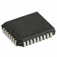
CY7C4241V-15JXC
Description
IC SYNC FIFO MEM 4KX9 32-PLCC
Manufacturer
Cypress Semiconductor Corp
Series
CY7Cr
Datasheet
1.CY7C4241V-15AXC.pdf
(18 pages)
Specifications of CY7C4241V-15JXC
Function
Synchronous
Memory Size
36K (4K x 9)
Data Rate
100MHz
Access Time
10ns
Voltage - Supply
3.3V
Operating Temperature
-40°C ~ 85°C
Mounting Type
Surface Mount
Package / Case
32-PLCC
Configuration
Dual
Density
36Kb
Access Time (max)
11ns
Word Size
9b
Organization
4Kx9
Sync/async
Synchronous
Expandable
Yes
Bus Direction
Uni-Directional
Clock Freq (max)
66.7MHz
Operating Supply Voltage (typ)
3.3V
Operating Supply Voltage (min)
3V
Operating Supply Voltage (max)
3.6V
Supply Current
20mA
Operating Temp Range
0C to 70C
Operating Temperature Classification
Commercial
Mounting
Surface Mount
Pin Count
32
Lead Free Status / RoHS Status
Lead free / RoHS Compliant
Available stocks
Company
Part Number
Manufacturer
Quantity
Price
Company:

Part Number:
CY7C4241V-15JXC
Manufacturer:
Cypress Semiconductor Corp
Quantity:
10 000
Company:
Part Number:
CY7C4241V-15JXCT
Manufacturer:
Cypress Semiconductor Corp
Quantity:
10 000


Document #: 38-06010 Rev. *B
Table 2. Status Flags
Width Expansion Configuration
Word width may be increased simply by connecting the corre-
sponding input control signals of multiple devices. A
composite flag should be created for each of the end-point
status flags (EF and FF). The partial status flags (PAE and
PAF) can be detected from any one device. Figure 2 demon-
strates a 18-bit word width by using two CY7C42X1Vs. Any
word
CY7C42X1Vs.
When the CY7C42X1V is in a Width Expansion Configuration,
the Read Enable (REN2) control input can be grounded (see
Figure 2). In this configuration, the Write Enable 2/Load
(WEN2/LD) pin is set to LOW at Reset so that the pin operates
as a control to load and read the programmable flag offsets.
Notes:
0
1 to n
(n+1) to 32
33 to (64−(m+1))
(64−m)
64
0
1 to n
(n+1) to 512
513 to (1024 −(m+1))
(1024−m)
1024
2. n = Empty Offset (n=7 default value).
3. m = Full Offset (m=7 default value).
CY7C4221V
[2]
[2]
width
[3]
CY7C4421V
to 63
[3]
to 1023
can
be
0
1 to n
(n+1) to 1024
1025 to (2048 −(m+1))
(2048−m)
2048
attained
[2]
CY7C4231V
0
1 to n
(n+1) to 128
129 to (256−(m+1))
(256−m)
256
[3]
Number of Words in FIFO
Number of Words in FIFO
to 2047
by
[2]
[3]
CY7C4201V
adding
to 255
0
1 to n
(n+1) to 2048
2049 to (4096 −(m+1))
(4096−m)
4096
additional
[2]
CY7C4241V
[3]
to 4095
0
1 to n
(n+1) to 256
257 to (512−(m+1))
(512−m)
512
Flag Operation
The CY7C42X1 devices provide four flag pins to indicate the
condition of the FIFO contents. Empty, Full, PAE, and PAF are
synchronous.
Full Flag
The Full Flag (FF) will go LOW when device is full. Write opera-
tions are inhibited whenever FF is LOW regardless of the state
of WEN1 and WEN2/LD. FF is synchronized to WCLK, i.e., it
is exclusively updated by each rising edge of WCLK.
Empty Flag
The Empty Flag (EF) will go LOW when the device is empty.
Read operations are inhibited whenever EF is LOW,
regardless of the state of REN1 and REN2. EF is synchronized
to RCLK, i.e., it is exclusively updated by each rising edge of
RCLK.
[2]
CY7C4421V/4201V/4211V/4221V
[3]
CY7C4211V
0
1 to n
(n+1) to 4096
4097 to (8192 −(m+1))
(8192−m)
8192
to 511
[2]
CY7C4251V
CY7C4231V/4241V/4251V
[3]
to 8191
FF
H
H
H
H
H
L
FF
H
H
H
H
H
L
PAF
H
H
H
H
L
L
PAF
H
H
H
H
L
L
PAE
Page 5 of 18
PAE
H
H
H
H
L
L
H
H
H
H
L
L
EF
EF
H
H
H
H
H
H
H
H
H
H
L
L
Related parts for CY7C4241V-15JXC
Image
Part Number
Description
Manufacturer
Datasheet
Request
R

Part Number:
Description:
IC SYNC FIFO MEM 4KX9 32-TQFP
Manufacturer:
Cypress Semiconductor Corp
Datasheet:

Part Number:
Description:
IC SYNC FIFO MEM 4KX9 32-PLCC
Manufacturer:
Cypress Semiconductor Corp
Datasheet:

Part Number:
Description:
Manufacturer:
Cypress Semiconductor Corp
Datasheet:
Part Number:
Description:
Manufacturer:
Cypress Semiconductor Corp
Datasheet:
Part Number:
Description:
IC SYNC FIFO MEM 4KX9 32-TQFP
Manufacturer:
Cypress Semiconductor Corp
Datasheet:
Part Number:
Description:
IC SYNC FIFO MEM 4KX9 32-PLCC
Manufacturer:
Cypress Semiconductor Corp
Datasheet:
Part Number:
Description:
IC SYNC FIFO MEM 4KX9 32-TQFP
Manufacturer:
Cypress Semiconductor Corp
Datasheet:
Part Number:
Description:
IC SYNC FIFO MEM 4KX9 32-TQFP
Manufacturer:
Cypress Semiconductor Corp
Datasheet:
Part Number:
Description:
IC SYNC FIFO MEM 4KX9 32-PLCC
Manufacturer:
Cypress Semiconductor Corp
Datasheet:
Part Number:
Description:
Manufacturer:
Cypress Semiconductor Corp
Datasheet:

Part Number:
Description:
Manufacturer:
Cypress Semiconductor Corp
Datasheet:
Part Number:
Description:
Manufacturer:
Cypress Semiconductor Corp
Datasheet:
Part Number:
Description:
Manufacturer:
Cypress Semiconductor Corp
Datasheet:
Part Number:
Description:
IC SYNC FIFO MEM 4KX9 32-PLCC
Manufacturer:
Cypress Semiconductor Corp
Datasheet:
Part Number:
Description:
IC SYNC FIFO MEM 4KX9 32-TQFP
Manufacturer:
Cypress Semiconductor Corp
Datasheet: