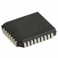
CY7C4241-15JXCT Cypress Semiconductor Corp, CY7C4241-15JXCT Datasheet - Page 3

CY7C4241-15JXCT
Manufacturer Part Number
CY7C4241-15JXCT
Description
IC SYNC FIFO MEM 4KX9 32-PLCC
Manufacturer
Cypress Semiconductor Corp
Series
CY7Cr
Specifications of CY7C4241-15JXCT
Function
Synchronous
Memory Size
36K (4K x 9)
Data Rate
100MHz
Access Time
10ns
Voltage - Supply
3.3V
Operating Temperature
-40°C ~ 85°C
Mounting Type
Surface Mount
Package / Case
32-PLCC
Configuration
Dual
Density
32Kb
Access Time (max)
15ns
Word Size
9b
Organization
4Kx9
Sync/async
Synchronous
Expandable
Yes
Bus Direction
Uni-Directional
Clock Freq (max)
40MHz
Operating Supply Voltage (typ)
5V
Operating Supply Voltage (min)
4.5V
Operating Supply Voltage (max)
5.5V
Supply Current
35mA
Operating Temp Range
0C to 70C
Operating Temperature Classification
Commercial
Mounting
Surface Mount
Pin Count
32
Lead Free Status / RoHS Status
Lead free / RoHS Compliant
Available stocks
Company
Part Number
Manufacturer
Quantity
Price
Company:
Part Number:
CY7C4241-15JXCT
Manufacturer:
Cypress Semiconductor Corp
Quantity:
10 000
Document #: 38-06016 Rev. *B
When the device is configured for programmable flags and
both WEN2/LD and WEN1 are LOW, the first LOW-to-HIGH
transition of WCLK writes data from the data inputs to the
empty offset least significant bit (LSB) register. The second,
third, and fourth LOW-to-HIGH transitions of WCLK store data
in the empty offset most significant bit (MSB) register, full offset
LSB register, and full offset MSB register, respectively, when
WEN2/LD and WEN1 are LOW. The fifth LOW-to-HIGH
transition of WCLK while WEN2/LD and WEN1 are LOW
writes data to the empty LSB register again. Figure 1 shows
the registers sizes and default values for the various device
types.
8
8
8
8
64 × 9
6 5
6 5
Empty Offset (LSB) Reg.
Default Value = 007h
Full Offset (LSB) Reg
Default Value = 007h
8
8
8
8
Empty Offset (LSB) Reg.
Default Value = 007h
Full Offset (LSB) Reg
Default Value = 007h
7
7
2K × 9
0
0
0
0
2
2
(MSB)
(MSB)
Figure 1. Offset Register Location and Default Values
000
000
8
8
8
8
256 × 9
Empty Offset (LSB) Reg.
Default Value = 007h
7
7
Full Offset (LSB) Reg
Default Value = 007h
0
0
0
0
8
8
8
8
Empty Offset (LSB) Reg.
Default Value = 007h
Full Offset (LSB) Reg
Default Value = 007h
7
7
0
0
0
0
4K × 9
3
It is not necessary to write to all the offset registers at one time.
A subset of the offset registers can be written; then by bringing
the WEN2/LD input HIGH, the FIFO is returned to normal
Read and Write operation. The next time WEN2/LD is brought
LOW, a Write operation stores data in the next offset register
in sequence.
The contents of the offset registers can be read to the data
outputs when WEN2/LD is LOW and both REN1 and REN2
are LOW. LOW-to-HIGH transitions of RCLK Read register
contents to the data outputs. Writes and reads should not be
preformed simultaneously on the offset registers.
3
(MSB)
(MSB)
0000
0000
8
8
8
8
512 × 9
Empty Offset (LSB) Reg.
Default Value = 007h
Full Offset (LSB) Reg
Default Value = 007h
7
7
0
0
0
0
CY7C4421/4201/4211/4221
1
1
(MSB)
(MSB)
0
0
8
8
8
8
CY7C4231/4241/4251
0
0
0
0
Empty Offset (LSB) Reg.
Default Value = 007h
Full Offset (LSB) Reg
Default Value = 007h
7
7
8K × 9
4
4
8
8
8
8
(MSB)
(MSB)
00000
00000
Empty Offset (LSB) Reg.
Default Value = 007h
Full Offset (LSB) Reg
Default Value = 007h
1K × 9
7
7
0
0
0
0
1
1
Page 3 of 18
(MSB)
(MSB)
00
00
0
0
0
0


