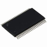
74LCX16374MTDX Fairchild Semiconductor, 74LCX16374MTDX Datasheet - Page 3

74LCX16374MTDX
Manufacturer Part Number
74LCX16374MTDX
Description
IC FLIP FLOP 16BIT D LV 48-TSSOP
Manufacturer
Fairchild Semiconductor
Series
74LCXr
Type
D-Type Busr
Datasheet
1.74LCX16374MTDX.pdf
(10 pages)
Specifications of 74LCX16374MTDX
Function
Standard
Output Type
Tri-State Non Inverted
Number Of Elements
2
Number Of Bits Per Element
8
Frequency - Clock
170MHz
Delay Time - Propagation
6.2ns
Trigger Type
Positive Edge
Current - Output High, Low
24mA, 24mA
Voltage - Supply
2 V ~ 3.6 V
Operating Temperature
-40°C ~ 85°C
Mounting Type
Surface Mount
Package / Case
48-TSSOP
Logic Family
LCX
Technology
CMOS
Number Of Bits
16
Number Of Elements
2
Clock-edge Trigger Type
Positive-Edge
Polarity
Non-Inverting
Operating Supply Voltage (typ)
2.5/3.3V
Package Type
TSSOP W
Propagation Delay Time
7.9ns
Low Level Output Current
24mA
High Level Output Current
-24mA
Frequency (max)
170MHz
Operating Supply Voltage (min)
2V
Operating Supply Voltage (max)
3.6V
Operating Temp Range
-40C to 85C
Operating Temperature Classification
Industrial
Mounting
Surface Mount
Pin Count
48
Lead Free Status / RoHS Status
Lead free / RoHS Compliant
Other names
74LCX16374MTDX
74LCX16374MTDXTR
74LCX16374MTDXTR
Available stocks
Company
Part Number
Manufacturer
Quantity
Price
Company:
Part Number:
74LCX16374MTDX
Manufacturer:
FAIRCHILD
Quantity:
1 758
Part Number:
74LCX16374MTDX
Manufacturer:
FAIRCHILD/ن»™ç«¥
Quantity:
20 000
Functional Description
The LCX16374 consists of sixteen edge-triggered flip-flops
with individual D-type inputs and 3-STATE true outputs.
The device is byte controlled with each byte functioning
identically, but independent of the other. The control pins
can be shorted together to obtain full 16-bit operation. Each
byte has a buffered clock and buffered Output Enable com-
mon to all flip-flops within that byte. The description which
follows applies to each byte. Each flip-flop will store the
Logic Diagrams
Please note that this diagram is provided only for the understanding of logic operations and should not be used to estimate propagation delays.
Byte 2 (8:15)
Byte 1 (0:7)
3
state of their individual D inputs that meet the setup and
hold time requirements on the LOW-to-HIGH Clock (CP
transition. With the Output Enable (OE
tents of the flip-flops are available at the outputs. When
OE
Operation of the OE
flip-flops.
n
is HIGH, the outputs go to the high impedance state.
n
input does not affect the state of the
www.fairchildsemi.com
n
) LOW, the con-
n
)


