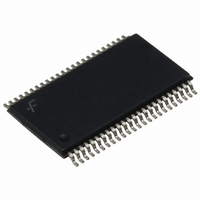
74LCX16374MTDX Fairchild Semiconductor, 74LCX16374MTDX Datasheet - Page 4

74LCX16374MTDX
Manufacturer Part Number
74LCX16374MTDX
Description
IC FLIP FLOP 16BIT D LV 48-TSSOP
Manufacturer
Fairchild Semiconductor
Series
74LCXr
Type
D-Type Busr
Datasheet
1.74LCX16374MTDX.pdf
(10 pages)
Specifications of 74LCX16374MTDX
Function
Standard
Output Type
Tri-State Non Inverted
Number Of Elements
2
Number Of Bits Per Element
8
Frequency - Clock
170MHz
Delay Time - Propagation
6.2ns
Trigger Type
Positive Edge
Current - Output High, Low
24mA, 24mA
Voltage - Supply
2 V ~ 3.6 V
Operating Temperature
-40°C ~ 85°C
Mounting Type
Surface Mount
Package / Case
48-TSSOP
Logic Family
LCX
Technology
CMOS
Number Of Bits
16
Number Of Elements
2
Clock-edge Trigger Type
Positive-Edge
Polarity
Non-Inverting
Operating Supply Voltage (typ)
2.5/3.3V
Package Type
TSSOP W
Propagation Delay Time
7.9ns
Low Level Output Current
24mA
High Level Output Current
-24mA
Frequency (max)
170MHz
Operating Supply Voltage (min)
2V
Operating Supply Voltage (max)
3.6V
Operating Temp Range
-40C to 85C
Operating Temperature Classification
Industrial
Mounting
Surface Mount
Pin Count
48
Lead Free Status / RoHS Status
Lead free / RoHS Compliant
Other names
74LCX16374MTDX
74LCX16374MTDXTR
74LCX16374MTDXTR
Available stocks
Company
Part Number
Manufacturer
Quantity
Price
Company:
Part Number:
74LCX16374MTDX
Manufacturer:
FAIRCHILD
Quantity:
1 758
Part Number:
74LCX16374MTDX
Manufacturer:
FAIRCHILD/ن»™ç«¥
Quantity:
20 000
www.fairchildsemi.com
V
V
V
I
T
'
V
V
V
I
I
I
I
I
T
V
V
V
V
I
I
I
Absolute Maximum Ratings
Note 4: The Absolute Maximum Ratings are those values beyond which the safety of the device cannot be guaranteed. The device should not be operated
at these limits. The parametric values defined in the Electrical Characteristics tables are not guaranteed at the Absolute Maximum Ratings. The “Recom-
mended Operating Conditions” table will define the conditions for actual device operation.
Note 5: I
Recommended Operating Conditions
OH
Note 6: Unused inputs must be held HIGH or LOW. They may not float.
DC Electrical Characteristics
IK
OK
O
CC
GND
I
OZ
OFF
Symbol
Symbol
A
t/
IH
IL
OH
OL
CC
I
O
STG
CC
I
O
Symbol
'
/I
V
OL
O
Absolute Maximum Rating must be observed.
Supply Voltage
Input Voltage
Output Voltage
Output Current
Free-Air Operating Temperature
Input Edge Rate, V
Supply Voltage
DC Input Voltage
DC Output Voltage
DC Input Diode Current
DC Output Diode Current
DC Output Source/Sink Current
DC Supply Current per Supply Pin
DC Ground Current per Ground Pin
Storage Temperature
HIGH Level Input Voltage
LOW Level Input Voltage
HIGH Level Output Voltage
LOW Level Output Voltage
Input Leakage Current
3-STATE Output Leakage
Power-Off Leakage Current
Parameter
Parameter
IN
0.8V – 2.0V, V
Parameter
(Note 4)
I
I
I
I
I
I
I
I
I
I
0
0
V
V
OH
OH
OH
OH
OH
OL
OL
OL
OL
OL
I
I
CC
d
d
or V
V
V
V
I
O
100
8 mA
12 mA
16 mA
24 mA
IH
d
O
100
8 mA
12 mA
18 mA
24 mA
d
0.5 to V
3.0V
5.5V
or V
5.5V
P
0.5 to
0.5 to
0.5 to
65 to
5.5V
A
P
IL
Value
A
r
r
r
Conditions
100
100
50
50
50
50
CC
4
150
7.0
7.0
7.0
(Note 6)
0.5
HIGH or LOW State
V
V
V
CC
CC
3-STATE
Output in HIGH or LOW State (Note 5)
V
V
V
CC
I
O
O
Data Retention
!
GND
3.0V
2.7V
2.3V
GND
V
Operating
CC
3-STATE
2.3
2.7
2.3
2.7
2.3
2.3
2.3
2.3
3.6V
3.0V
2.7V
V
(V)
2.3
2.7
3.0
3.0
2.3
2.7
3.0
3.0
0
CC
Conditions
2.7
3.6
2.7
3.6
3.6
3.6
3.6
3.6
Min
2.0
1.5
V
0
0
0
40
0
T
CC
A
Min
1.7
2.0
1.8
2.2
2.4
2.2
0.2
40
q
C to
Max
V
r
r
3.6
3.6
5.5
5.5
r
85
10
CC
24
12
8
Max
0.55
r
r
0.7
0.8
0.2
0.6
0.4
0.4
10
85
5.0
5.0
q
C
Units
ns/V
Units
mA
q
Units
V
V
V
mA
mA
mA
mA
mA
C
q
P
P
P
V
V
V
C
V
V
V
V
A
A
A


