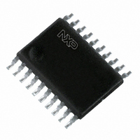
74LVC273PW,112 NXP Semiconductors, 74LVC273PW,112 Datasheet - Page 10

74LVC273PW,112
Manufacturer Part Number
74LVC273PW,112
Description
IC OCT D-TYPE FLIP-FLOP 20TSSOP
Manufacturer
NXP Semiconductors
Series
74LVCr
Type
D-Type Busr
Datasheet
1.74LVC273PW118.pdf
(18 pages)
Specifications of 74LVC273PW,112
Output Type
Non-Inverted
Package / Case
20-TSSOP
Function
Master Reset
Number Of Elements
1
Number Of Bits Per Element
8
Frequency - Clock
150MHz
Delay Time - Propagation
1.5ns
Trigger Type
Positive Edge
Current - Output High, Low
24mA, 24mA
Voltage - Supply
2.7 V ~ 3.6 V
Operating Temperature
-40°C ~ 125°C
Mounting Type
Surface Mount
Number Of Circuits
8
Logic Family
74LVC
Logic Type
D-Type Flip-Flop
Polarity
Non-Inverting
Input Type
Single-Ended
Propagation Delay Time
4.8 ns
High Level Output Current
- 24 mA
Low Level Output Current
24 mA
Supply Voltage (max)
3.6 V
Maximum Operating Temperature
+ 125 C
Mounting Style
SMD/SMT
Minimum Operating Temperature
- 40 C
Supply Voltage (min)
1.2 V
Lead Free Status / RoHS Status
Lead free / RoHS Compliant
Lead Free Status / RoHS Status
Lead free / RoHS Compliant, Lead free / RoHS Compliant
Other names
568-2302-5
74LVC273PW
935210650112
74LVC273PW
935210650112
Philips Semiconductors
AC WAVEFORMS
2004 Mar 12
handbook, full pagewidth
handbook, full pagewidth
Octal D-type flip-flop with reset;
positive-edge trigger
V
V
V
Fig.5
V
V
Fig.6
M
M
OL
M
M
= 1.5 V at V
= 0.5V
= 1.5 V at V
= 0.5V
and V
CC
Clock (CP) to output (Qn) propagation delays, the clock pulse width and the maximum clock pulse
frequency.
CC
Master reset (MR) pulse width, the master reset to output (Qn) propagation delays and the master reset
to clock (CP) removal time.
OH
at V
at V
are typical output voltage drop that occur with the output load.
CC
CC
CC
CC
< 2.7 V.
< 2.7 V.
2.7 V.
2.7 V.
Qn output
MR input
CP input
Qn output
CP input
GND
GND
V I
V I
GND
V OH
V OL
V I
V M
t PHL
t W
V M
V M
1/f max
10
t PLH
t W
V M
t PLH
V M
t rem
V M
MNA765
MNA464
Product specification
74LVC273


