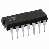
74HCT74N,652 NXP Semiconductors, 74HCT74N,652 Datasheet - Page 13

74HCT74N,652
Manufacturer Part Number
74HCT74N,652
Description
IC FLIP FLOP DUAL D TYPE 14DIP
Manufacturer
NXP Semiconductors
Series
74HCTr
Type
D-Typer
Datasheet
1.74HC74BQ115.pdf
(22 pages)
Specifications of 74HCT74N,652
Package / Case
14-DIP (0.300", 7.62mm)
Function
Set(Preset) and Reset
Output Type
Differential
Number Of Elements
2
Number Of Bits Per Element
1
Frequency - Clock
18MHz
Delay Time - Propagation
18ns
Trigger Type
Positive Edge
Current - Output High, Low
4mA, 4mA
Voltage - Supply
4.5 V ~ 5.5 V
Operating Temperature
-40°C ~ 125°C
Mounting Type
Through Hole
Number Of Circuits
2
Logic Family
74HCT
Logic Type
D-Type Flip-Flop
Polarity
Inverting/Non-Inverting
Input Type
Single-Ended
Propagation Delay Time
18 ns
High Level Output Current
- 4 mA
Supply Voltage (max)
5.5 V
Maximum Operating Temperature
+ 125 C
Mounting Style
SMD/SMT
Minimum Operating Temperature
- 40 C
Supply Voltage (min)
4.5 V
Technology
CMOS
Number Of Bits
2
Number Of Elements
2
Clock-edge Trigger Type
Positive-Edge
Operating Supply Voltage (typ)
5V
Package Type
PDIP
Low Level Output Current
4mA
Frequency (max)
18MHz
Operating Supply Voltage (min)
4.5V
Operating Supply Voltage (max)
5.5V
Operating Temp Range
-40C to 125C
Operating Temperature Classification
Automotive
Mounting
Through Hole
Pin Count
14
Lead Free Status / RoHS Status
Lead free / RoHS Compliant
Lead Free Status / RoHS Status
Lead free / RoHS Compliant, Lead free / RoHS Compliant
Other names
568-1566-5
74HCT74N
933669250652
74HCT74N
933669250652
Philips Semiconductors
AC WAVEFORMS
2003 Jul 10
handbook, full pagewidth
Dual D-type flip-flop with set and reset;
positive-edge trigger
The shaded areas indicate when the input is permitted to change for predictable output performance.
74HC74: V
74HCT74: V
Fig.7
The clock (nCP) to output (nQ, nQ) propagation delays, the clock pulse width, the nD to nCP set-up,
the nCP to nD hold times, the output transition times and the maximum clock pulse frequency.
M
M
= 50%; V
= 1.3 V; V
I
= GND to V
I
= GND to 3 V.
nCP input
nQ output
nQ output
nD input
CC
.
GND
GND
V OH
V OH
V OL
V OL
V I
V I
V M
t PLH
t su
t h
V M
13
V M
t W
V M
t PHL
1/f max
t PHL
t su
t h
t PLH
MNA422
74HC74; 74HCT74
Product specification


