74HCT74N,652 NXP Semiconductors, 74HCT74N,652 Datasheet - Page 4
74HCT74N,652
Manufacturer Part Number
74HCT74N,652
Description
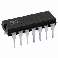
IC FLIP FLOP DUAL D TYPE 14DIP
Manufacturer
NXP Semiconductors
Series
74HCTr
Type
D-Typer
Datasheet
1.74HC74BQ115.pdf
(22 pages)
Specifications of 74HCT74N,652
Package / Case
14-DIP (0.300", 7.62mm)
Function
Set(Preset) and Reset
Output Type
Differential
Number Of Elements
2
Number Of Bits Per Element
1
Frequency - Clock
18MHz
Delay Time - Propagation
18ns
Trigger Type
Positive Edge
Current - Output High, Low
4mA, 4mA
Voltage - Supply
4.5 V ~ 5.5 V
Operating Temperature
-40°C ~ 125°C
Mounting Type
Through Hole
Number Of Circuits
2
Logic Family
74HCT
Logic Type
D-Type Flip-Flop
Polarity
Inverting/Non-Inverting
Input Type
Single-Ended
Propagation Delay Time
18 ns
High Level Output Current
- 4 mA
Supply Voltage (max)
5.5 V
Maximum Operating Temperature
+ 125 C
Mounting Style
SMD/SMT
Minimum Operating Temperature
- 40 C
Supply Voltage (min)
4.5 V
Technology
CMOS
Number Of Bits
2
Number Of Elements
2
Clock-edge Trigger Type
Positive-Edge
Operating Supply Voltage (typ)
5V
Package Type
PDIP
Low Level Output Current
4mA
Frequency (max)
18MHz
Operating Supply Voltage (min)
4.5V
Operating Supply Voltage (max)
5.5V
Operating Temp Range
-40C to 125C
Operating Temperature Classification
Automotive
Mounting
Through Hole
Pin Count
14
Lead Free Status / RoHS Status
Lead free / RoHS Compliant
Lead Free Status / RoHS Status
Lead free / RoHS Compliant, Lead free / RoHS Compliant
Other names
568-1566-5
74HCT74N
933669250652
74HCT74N
933669250652


Philips Semiconductors
PINNING
2003 Jul 10
handbook, halfpage
Dual D-type flip-flop with set and reset;
positive-edge trigger
Fig.1
PIN
10
11
12
13
14
1
2
3
4
5
6
7
8
9
Pin configuration DIP14, SO14 and
(T)SSOP14.
GND
1RD
1CP
1SD
1Q
1Q
1D
1RD
1D
1CP
1SD
1Q
1Q
GND
2Q
2Q
2SD
2CP
2D
2RD
V
CC
1
2
3
4
5
6
7
SYMBOL
74
MNA417
asynchronous reset-direct input (active LOW)
data input
clock input (LOW-to-HIGH, edge-triggered)
asynchronous set-direct input (active LOW)
true flip-flop output
complement flip-flop output
ground (0 V)
complement flip-flop output
true flip-flop output
asynchronous set-direct input (active LOW)
clock input (LOW-to-HIGH, edge-triggered)
data input
asynchronous reset-direct input (active LOW)
positive supply voltage
14
13
12
11
10
9
8
V CC
2RD
2D
2CP
2SD
2Q
2Q
4
handbook, halfpage
(1) The die substrate is attached to this pad using conductive die
attach material. It can not be used as a supply pin or input.
DESCRIPTION
Fig.2 Pin configuration DHVQFN14.
1CP
1SD
1D
1Q
1Q
Top view
2
3
4
5
6
GND
1RD
7
1
GND
74HC74; 74HCT74
V CC
(1)
2Q
14
8
Product specification
MNB038
13
12
11
10
9
2RD
2D
2CP
2SD
2Q
Related parts for 74HCT74N,652
Image
Part Number
Description
Manufacturer
Datasheet
Request
R

Part Number:
Description:
Flip Flop D-Type Pos-Edge 2-Element 14-Pin PDIP Bulk
Manufacturer:
NXP Semiconductors
Datasheet:

Part Number:
Description:
IC BUFF/DVR TRI-ST DUAL 20DIP
Manufacturer:
Fairchild Semiconductor
Datasheet:

Part Number:
Description:
IC BUS TRANSCVR 3-ST 8BIT 20DIP
Manufacturer:
ON Semiconductor
Datasheet:

Part Number:
Description:
IC TRANSCEIVER 3-ST 8BIT 20SOIC
Manufacturer:
Fairchild Semiconductor
Datasheet:

Part Number:
Description:
IC BUFFER NONINV QUAD 3ST 14SOIC
Manufacturer:
ON Semiconductor
Datasheet:
Part Number:
Description:
IC BUFFER NONINV QUAD 3ST 14SOIC
Manufacturer:
ON Semiconductor
Datasheet:

Part Number:
Description:
IC BUS TRANSCVR 3-ST 8BIT 20SOIC
Manufacturer:
ON Semiconductor
Datasheet:

Part Number:
Description:
IC BUFF/DVR TRI-ST 8BIT 20SOIC
Manufacturer:
ON Semiconductor
Datasheet:

Part Number:
Description:
IC FLIP FLOP OCT D 3ST 20TSSOP
Manufacturer:
Fairchild Semiconductor
Datasheet:

Part Number:
Description:
IC FLIP FLOP OCTAL D 20-DIP
Manufacturer:
STMicroelectronics
Datasheet:

Part Number:
Description:
IC FLIP FLOP DUAL D-TYPE 14-SOIC
Manufacturer:
Fairchild Semiconductor
Datasheet:
Part Number:
Description:
IC FLIP FLOP OCTAL D 20-SOIC
Manufacturer:
Fairchild Semiconductor
Datasheet:

Part Number:
Description:
IC FLIP FLOP OCT D 3ST 20-SOIC
Manufacturer:
ON Semiconductor
Datasheet:

Part Number:
Description:
IC INVERT HEX SCHM TRIG 14-SOIC
Manufacturer:
ON Semiconductor
Datasheet:

Part Number:
Description:
IC INVERTER HEX LSTTL IN 14TSSOP
Manufacturer:
ON Semiconductor
Datasheet: