MC14175BCPG ON Semiconductor, MC14175BCPG Datasheet - Page 2
MC14175BCPG
Manufacturer Part Number
MC14175BCPG
Description
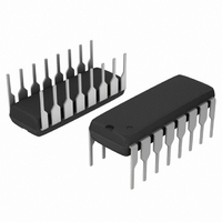
IC FLIP FLOP QUAD TYPE D 16-DIP
Manufacturer
ON Semiconductor
Series
4000Br
Type
D-Type Busr
Specifications of MC14175BCPG
Function
Reset
Output Type
Differential
Number Of Elements
1
Number Of Bits Per Element
4
Frequency - Clock
14MHz
Delay Time - Propagation
70ns
Trigger Type
Positive Edge
Current - Output High, Low
8mA, 8mA
Voltage - Supply
3 V ~ 18 V
Operating Temperature
-55°C ~ 125°C
Mounting Type
Through Hole
Package / Case
16-DIP (0.300", 7.62mm)
Logic Family
4000
Technology
CMOS
Number Of Bits
4
Number Of Elements
1
Clock-edge Trigger Type
Positive-Edge
Polarity
Invert/Non-Invert
Operating Supply Voltage (typ)
3.3/5/9/12/15V
Package Type
PDIP
Propagation Delay Time
500ns
Low Level Output Current
4.2mA
High Level Output Current
-4.2mA
Frequency (max)
6.5MHz
Operating Supply Voltage (min)
3V
Operating Supply Voltage (max)
18V
Operating Temp Range
-55C to 125C
Operating Temperature Classification
Military
Mounting
Through Hole
Pin Count
16
Circuit Type
Low-Power Schottky
Current, Supply
600 μA
Function Type
4-Channels, D-Type
Logic Function
Flip-Flop
Logic Type
CMOS
Number Of Circuits
Quad
Special Features
Buffered Output
Temperature, Operating, Range
-55 to +125 °C
Voltage, Supply
3 to 18 VDC
Lead Free Status / RoHS Status
Lead free / RoHS Compliant
Other names
MC14175BCPG
MC14175BCPGOS
MC14175BCPGOS


X = Don’t Care
TRUTH TABLE
Clock
X
Inputs
Data
X
X
0
1
Figure 1. Pin Assignment
Reset
1
1
1
0
V
Q0
Q0
D0
D1
Q1
Q1
SS
R
1
2
3
4
5
6
7
8
Q
Q
0
1
0
Outputs
Figure 4. Functional Block Diagram
16
15
14
13
12
11
10
9
Figure 3. Timing Diagram
V
Q3
Q3
D3
D2
Q2
Q2
C
Q
Q
1
0
1
DD
http://onsemi.com
No
Change
MC14175B
2
12
13
Figure 2. Block Diagram
9
1
4
5
CLOCK
RESET
D0
D1
D2
D3
V
V
DD
SS
= PIN 8
= PIN 16
Q0
Q0
Q1
Q1
Q2
Q2
Q3
Q3
2
3
7
6
10
11
15
14
Related parts for MC14175BCPG
Image
Part Number
Description
Manufacturer
Datasheet
Request
R

Part Number:
Description:
CONTACTOR, 1NO, 110VAC, 14A, DIN RAIL
Manufacturer:
IMO PRECISION CONTROLS
Datasheet:
Part Number:
Description:
CONTACTOR, 1NO, 230VAC, 14A, DIN RAIL
Manufacturer:
IMO PRECISION CONTROLS
Datasheet:
Part Number:
Description:
CONTACTOR, 1NO, 24VAC, 14A, DIN RAIL
Manufacturer:
IMO PRECISION CONTROLS
Datasheet:

Part Number:
Description:
ON Semiconductor [VOLTAGE REGULATOR]
Manufacturer:
ON Semiconductor
Datasheet:
Part Number:
Description:
357-036-542-201 CARDEDGE 36POS DL .156 BLK LOPRO
Manufacturer:
ON Semiconductor
Datasheet:
Part Number:
Description:
357-036-542-201 CARDEDGE 36POS DL .156 BLK LOPRO
Manufacturer:
ON Semiconductor
Datasheet:
Part Number:
Description:
357-036-542-201 CARDEDGE 36POS DL .156 BLK LOPRO
Manufacturer:
ON Semiconductor
Datasheet:
Part Number:
Description:
357-036-542-201 CARDEDGE 36POS DL .156 BLK LOPRO
Manufacturer:
ON Semiconductor
Datasheet:
Part Number:
Description:
357-036-542-201 CARDEDGE 36POS DL .156 BLK LOPRO
Manufacturer:
ON Semiconductor
Datasheet:
Part Number:
Description:
357-036-542-201 CARDEDGE 36POS DL .156 BLK LOPRO
Manufacturer:
ON Semiconductor
Datasheet:
Part Number:
Description:
357-036-542-201 CARDEDGE 36POS DL .156 BLK LOPRO
Manufacturer:
ON Semiconductor
Datasheet:
Part Number:
Description:
357-036-542-201 CARDEDGE 36POS DL .156 BLK LOPRO
Manufacturer:
ON Semiconductor
Datasheet:
Part Number:
Description:
357-036-542-201 CARDEDGE 36POS DL .156 BLK LOPRO
Manufacturer:
ON Semiconductor
Datasheet:
Part Number:
Description:
357-036-542-201 CARDEDGE 36POS DL .156 BLK LOPRO
Manufacturer:
ON Semiconductor
Datasheet: