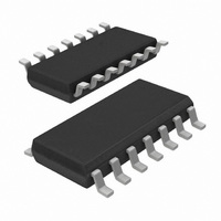
N74F5074D,602 NXP Semiconductors, N74F5074D,602 Datasheet - Page 2

N74F5074D,602
Manufacturer Part Number
N74F5074D,602
Description
IC FLIP FLOP/CLOCK DRIVER 14SOIC
Manufacturer
NXP Semiconductors
Series
74Fr
Type
D-Typer
Datasheet
1.N74F5074D602.pdf
(12 pages)
Specifications of N74F5074D,602
Function
Set(Preset) and Reset
Output Type
Differential
Number Of Elements
2
Number Of Bits Per Element
1
Frequency - Clock
120MHz
Trigger Type
Positive Edge
Current - Output High, Low
15mA, 20mA
Voltage - Supply
4.5 V ~ 5.5 V
Operating Temperature
0°C ~ 70°C
Mounting Type
Surface Mount
Package / Case
14-SOIC (3.9mm Width), 14-SOL
Lead Free Status / RoHS Status
Lead free / RoHS Compliant
Delay Time - Propagation
-
Other names
568-1732-5
935007610602
N74F5074D
935007610602
N74F5074D
Philips Semiconductors
FEATURES
ORDERING INFORMATION
INPUT AND OUTPUT LOADING
AND FAN OUT TABLE
NOTE: One (1.0) FAST unit load is defined as: 20 A in the high
state and 0.6mA in the low state.
Q0, Q1, Q0,
September 14, 1990
14–pin plastic DIP
14–pin plastic SO
Metastable immune characteristics
Output skew guaranteed less than 1.5ns
High source current (I
applications
Pin out compatible with 74F74
74F50728 for synchronizing cascaded D–type flip–flop
See 74F50729 for synchronizing dual D–type flip–flop with
edge–triggered set and reset
See 74F50109 for synchronizing dual J–K positive
edge–triggered flip–flop
Industrial temperature range available (–40 C to +85 C)
RD0, RD1
CP0, CP1
SD0, SD1
Synchronizing dual D-type flip-flop/clock driver
DESCRIPTION
74F5074
D0, D1
TYPE
PINS
Q1
Data inputs
Clock inputs (active
rising edge)
Set inputs (active low)
Reset inputs (active
low)
Data outputs
TYPICAL f
DESCRIPTION
120MHz
COMMERCIAL RANGE
OH
T
amb
V
= 15mA) ideal for clock driver
ORDER CODE
CC
max
N74F5074N
N74F5074D
= 0 C to +70 C
= 5V 10%,
1.0/0.417
CURRENT (TOTAL)
1.0/1.0
1.0/1.0
1.0/1.0
750/33
TYPICAL SUPPLY
HIGH/
(U.L.)
LOW
74F
20mA
PKG DWG #
SOT108-1
SOT27-1
20 A/250 A
15mA/20mA
LOAD VAL-
20 A/20 A
20 A/20 A
20 A/20 A
UE HIGH/
LOW
2
PIN CONFIGURATION
IEC/IEEE SYMBOL
LOGIC SYMBOL
V
GND = Pin 7
CC
= Pin 14
10
11
12
13
10
13
4
3
2
1
11
3
4
1
GND
CP0
RD0
SD0
Q0
Q0
D0
1
2
3
4
5
6
7
CP0
SD0
RD0
CP1
SD1
RD1
S
2D
S
R
1D
R
Q0 Q0 Q1 Q1
C1
5
C2
D0
6
2
&
12
D1
9
SF00582
SF00583
14
13
12
11
10
8
9
8
CP1
D1
SD1
Q1
V
RD1
Q1
CC
SF00584
Product specification
74F5074
3
6
9
8
853-1391 00419


