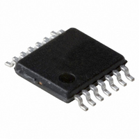
74LV74PW,118 NXP Semiconductors, 74LV74PW,118 Datasheet - Page 7

74LV74PW,118
Manufacturer Part Number
74LV74PW,118
Description
IC DUAL D FF POSEDG TRIG 14TSSOP
Manufacturer
NXP Semiconductors
Series
74LVr
Type
D-Typer
Specifications of 74LV74PW,118
Output Type
Differential
Package / Case
14-TSSOP
Function
Set(Preset) and Reset
Number Of Elements
2
Number Of Bits Per Element
1
Frequency - Clock
56MHz
Trigger Type
Positive Edge
Current - Output High, Low
12mA, 12mA
Voltage - Supply
1 V ~ 5.5 V
Operating Temperature
-40°C ~ 125°C
Mounting Type
Surface Mount
Number Of Circuits
2
Logic Family
LV
Logic Type
D-Type Edge Triggered Flip-Flop
Polarity
Inverting/Non-Inverting
Input Type
Single-Ended
Propagation Delay Time
11 ns at 3.3 V
High Level Output Current
- 12 mA
Low Level Output Current
12 mA
Supply Voltage (max)
5.5 V
Maximum Operating Temperature
+ 125 C
Mounting Style
SMD/SMT
Minimum Operating Temperature
- 40 C
Supply Voltage (min)
1 V
Delay Time - Propagation
-
Technology
CMOS
Number Of Bits
2
Number Of Elements
2
Clock-edge Trigger Type
Positive-Edge
Operating Supply Voltage (typ)
3.3V
Package Type
TSSOP
Frequency (max)
56MHz
Operating Supply Voltage (min)
1V
Operating Supply Voltage (max)
5.5V
Operating Temp Range
-40C to 125C
Operating Temperature Classification
Automotive
Mounting
Surface Mount
Pin Count
14
Lead Free Status / RoHS Status
Lead free / RoHS Compliant
Delay Time - Propagation
-
Lead Free Status / Rohs Status
Lead free / RoHS Compliant
Other names
74LV74PW-T
74LV74PW-T
935175140118
74LV74PW-T
935175140118
Philips Semiconductors
AC WAVEFORMS
V
V
V
output load.
NOTE:
The shaded areas indicate when the input is permitted to change for
predictable output performance.
1998 Apr 20
propagation delays, the set and reset pulse widths and the nR
Figure 2.The set (nS
M
M
OL
delays, the clock pulse width, the nD to nCP setup times, the
Dual D-type flip-flop with set and reset;
positive edge-trigger
nQ OUTPUT
nQ OUTPUT
= 1.5V at V
= 0.5 * V
nCP to nD hold times, the output transition times and the
Figure 1.The clock (nCP) to output (nQ, nQ) propagation
nCP INPUT
and V
nD INPUT
nQ OUTPUT
nQ OUTPUT
nCP INPUT
nS
nR
GND
GND
D
D
V
V
V
V
OH
OH
OH
INPUT
INPUT
OL
OL
V
Ï Ï Ï
Ï Ï Ï
V
CC
GND
GND
GND
I
I
V
V
V
V
are the typical output voltage drop that occur with the
OH
OH
OL
OL
CC
V
V
V
at V
I
I
I
maximum clock pulse frequency
w 2.7V v 3.6V
CC
VM
D
t 2.7V and w 4.5V
V
to nCP removal time
t
) and reset (nR
su
M
t
V
V
W
t
M
M
t
PHL
t
Ï Ï Ï Ï
Ï Ï Ï Ï
PLH
PHL
t
h
V
M
t
W
V
V
t
M
M
PLH
1/f
D
max
) input to output (nQ, nQ)
V
t
M
su
t
Ï Ï Ï
Ï Ï Ï
W
t
t
PHL
PLH
t
h
SV00335
SV00336
t
t
PLH
PHL
V
t
M
rem
D
7
TEST CIRCUIT
t
PLH/
GENERATOR
TEST
DEFINITIONS
R
C
R
T
PULSE
L
L
t
PHL
= Load resistor
= Load capacitance includes jig and probe capacitiance
= Termination resistance should be equal to Z
Figure 3. Load circuitry for switching times
Test Circuit for Outputs
V
2.7–3.6V
l
< 2.7V
R
V
4.5 V
T
CC
D.U.T.
V
cc
2.7V
V
V
V
CC
CC
I
V
O
OUT
C
L
of pulse generators.
Product specification
50pF
74LV74
SV00902
R
L
= 1k


