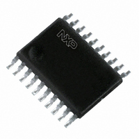
74HC374PW,112 NXP Semiconductors, 74HC374PW,112 Datasheet - Page 2

74HC374PW,112
Manufacturer Part Number
74HC374PW,112
Description
IC OCT D FF POS-EDG TRIG 20TSSOP
Manufacturer
NXP Semiconductors
Series
74HCr
Type
D-Type Busr
Datasheet
1.74HC374N652.pdf
(8 pages)
Specifications of 74HC374PW,112
Function
Standard
Output Type
Tri-State Non Inverted
Number Of Elements
1
Number Of Bits Per Element
8
Frequency - Clock
83MHz
Delay Time - Propagation
14ns
Trigger Type
Positive Edge
Voltage - Supply
2 V ~ 6 V
Operating Temperature
-40°C ~ 125°C
Mounting Type
Surface Mount
Package / Case
20-TSSOP
Lead Free Status / RoHS Status
Lead free / RoHS Compliant
Current - Output High, Low
-
Other names
74HC374PW
74HC374PW
935174860112
74HC374PW
935174860112
Philips Semiconductors
FEATURES
GENERAL DESCRIPTION
The 74HC/HCT374 are high-speed Si-gate CMOS devices
and are pin compatible with low power Schottky TTL
(LSTTL). They are specified in compliance with JEDEC
standard no. 7A.
QUICK REFERENCE DATA
GND = 0 V; T
Notes
1. C
2. For HC the condition is V
ORDERING INFORMATION
See
December 1990
t
f
C
C
PHL
max
3-state non-inverting outputs for bus oriented
applications
8-bit positive, edge-triggered register
Common 3-state output enable input
Independent register and 3-state buffer operation
Output capability: bus driver
I
Octal D-type flip-flop; positive
edge-trigger; 3-state
I
PD
CC
SYMBOL
f
f
C
V
For HCT the condition is V
i
o
“74HC/HCT/HCU/HCMOS Logic Package Information”
/ t
CC
PD
L
category: MSI
= output frequency in MHz
= input frequency in MHz
(C
PLH
= output load capacitance in pF
P
is used to determine the dynamic power dissipation (P
= supply voltage in V
L
D
= C
V
amb
CC
PD
2
= 25 C; t
propagation delay CP to Q
maximum clock frequency
input capacitance
power dissipation capacitance per flip-flop
V
f
o
CC
) = sum of outputs
2
f
r
i
= t
I
I
f
= GND to V
= GND to V
= 6 ns
(C
PARAMETER
L
V
CC
2
CC
CC
n
f
o
) where:
1.5 V
2
.
The 74HC/HCT374 are octal D-type flip-flops featuring
separate D-type inputs for each flip-flop and 3-state
outputs for bus oriented applications. A clock (CP) and an
output enable (OE) input are common to all flip-flops.
The 8 flip-flops will store the state of their individual
D-inputs that meet the set-up and hold times requirements
on the LOW-to-HIGH CP transition.
When OE is LOW, the contents of the 8 flip-flops are
available at the outputs. When OE is HIGH, the outputs go
to the high impedance OFF-state. Operation of the
OE input does not affect the state of the flip-flops.
The “374” is functionally identical to the “534”, but has
non-inverting outputs.
D
C
notes 1 and 2
in W):
L
= 15 pF; V
CONDITIONS
CC
= 5 V
74HC/HCT374
15
77
3.5
17
Product specification
HC
TYPICAL
13
48
3.5
17
HCT
ns
MHz
pF
pF
UNIT


