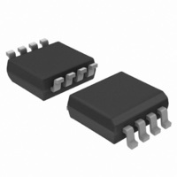
74AUP2G80DC,125 NXP Semiconductors, 74AUP2G80DC,125 Datasheet - Page 4

74AUP2G80DC,125
Manufacturer Part Number
74AUP2G80DC,125
Description
IC DUAL D-TYPE F-F 8-VSSOP
Manufacturer
NXP Semiconductors
Series
74AUPr
Type
D-Typer
Datasheet
1.74AUP2G80GD125.pdf
(24 pages)
Specifications of 74AUP2G80DC,125
Function
Standard
Output Type
Inverted
Number Of Elements
2
Number Of Bits Per Element
1
Frequency - Clock
550MHz
Delay Time - Propagation
2.2ns
Trigger Type
Positive Edge
Current - Output High, Low
4mA, 4mA
Voltage - Supply
0.8 V ~ 3.6 V
Operating Temperature
-40°C ~ 125°C
Mounting Type
Surface Mount
Package / Case
US8, 8-VSSOP
Lead Free Status / RoHS Status
Lead free / RoHS Compliant
Other names
74AUP2G80DC-G
74AUP2G80DC-G
935280722125
74AUP2G80DC-G
935280722125
NXP Semiconductors
Table 3.
7. Functional description
Table 4.
[1]
74AUP2G80
Product data sheet
Symbol
1CP, 2CP
1D, 2D
GND
1Q, 2Q
V
Input
nCP
↑
↑
L
Fig 6.
CC
H = HIGH voltage level;
L = LOW voltage level;
↑ = LOW-to-HIGH CP transition;
X = don’t care;
q = lower case letter indicates the state of referenced input, one setup time prior to the LOW-to-HIGH CP transition.
Pin configuration SOT996-2
GND
Pin description
Function table
1CP
2Q
1D
Pin
SOT765-1, SOT833-1, SOT1089,
SOT996-2, SOT1116 and SOT1203
1, 5
2, 6
4
7, 3
8
1
2
3
4
6.2 Pin description
Transparent top view
74AUP2G80
[1]
001aai216
nD
L
H
X
All information provided in this document is subject to legal disclaimers.
8
7
6
5
V
1Q
2D
2CP
CC
Rev. 5 — 5 October 2010
Low-power dual D-type flip-flop; positive-edge trigger
SOT902-1
7, 3
6, 2
4
1, 5
8
Fig 7.
Pin configuration SOT902-1
terminal 1
index area
2CP
1Q
2D
Description
clock input
data input
ground (0 V)
data output
supply voltage
Output
nQ
H
L
q
1
2
3
Transparent top view
74AUP2G80
74AUP2G80
© NXP B.V. 2010. All rights reserved.
7
6
5
001aaf310
1CP
1D
2Q
4 of 24


