74LVCH162374ADGG,5 NXP Semiconductors, 74LVCH162374ADGG,5 Datasheet - Page 2
74LVCH162374ADGG,5
Manufacturer Part Number
74LVCH162374ADGG,5
Description
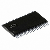
IC 16BIT EDGE TRIG D FF 48TSSOP
Manufacturer
NXP Semiconductors
Series
74LVCHr
Type
D-Type Busr
Datasheet
1.74LVCH162374ADGG5.pdf
(17 pages)
Specifications of 74LVCH162374ADGG,5
Function
Standard
Output Type
Tri-State Non Inverted
Number Of Elements
2
Number Of Bits Per Element
8
Frequency - Clock
150MHz
Delay Time - Propagation
1.5ns
Trigger Type
Positive Edge
Current - Output High, Low
12mA, 12mA
Voltage - Supply
1.2 V ~ 3.6 V
Operating Temperature
-40°C ~ 125°C
Mounting Type
Surface Mount
Package / Case
48-TSSOP
Lead Free Status / RoHS Status
Lead free / RoHS Compliant
Other names
74LVCH162374ADG
74LVCH162374ADG
935238770512
74LVCH162374ADG
935238770512


Philips Semiconductors
FEATURES
DESCRIPTION
The 74LVCH162374A is a 16-bit edge triggered flip-flop
featuring separate D-type inputs for each flip-flop and
QUICK REFERENCE DATA
GND = 0 V; T
Notes
1. C
2. The condition is V
2004 May 19
t
t
t
f
C
C
PHL
PZH
PHZ
max
5 V tolerant inputs/outputs for interfacing with 5 V logic
Wide supply voltage range from 1.2 V to 3.6 V
CMOS low power consumption
MULTIBYTE flow-through standard pin-out architecture
Low inductance multiple power and ground pins for
minimum noise and ground bounce
Direct interface with TTL levels
All data inputs have bushold
High-impedance outputs when V
Complies with JEDEC standard JESD8-B/JESD36
ESD protection:
– HBM EIA/JESD22-A114-B exceeds 2000 V
– MM EIA/JESD22-A115-A exceeds 200 V.
Specified from 40 C to +85 C and 40 C to +125 C.
I
PD
16-bit edge triggered D-type flip-flop with 30
termination resistors; 5 V input/output tolerant; 3-state
SYMBOL
P
f
f
C
V
N = total load switching outputs;
i
o
/t
/t
/t
(C
D
CC
PD
= input frequency in MHz;
L
PLH
PZL
PLZ
= output frequency in MHz;
= output load capacitance in pF;
= C
L
is used to determine the dynamic power dissipation (P
= supply voltage in Volts;
PD
V
CC
amb
2
V
CC
= 25 C; t
propagation delay nCP to nQn
3-state output enable time nOE to nQn C
3-state output disable time nOE to nQn C
maximum clock frequency
input capacitance
power dissipation capacitance per
flip-flop
f
o
2
) = sum of the outputs.
I
f
= GND to V
i
N + (C
r
= t
PARAMETER
f
2.5 ns.
L
CC
CC
.
= 0 V
V
CC
2
f
o
) where:
C
V
2
CC
L
L
L
outputs enabled
outputs disabled
3-state outputs for bus oriented applications. The
74LVCH162374A consists of 2 sections of eight
edge-triggered flip-flops. A clock (CP) input and an output
enable (OE) are provided for each octal. Inputs can be
driven from either 3.3 V or 5 V devices. In 3-state
operation, outputs can handle 5 V. These features allow
the use of these devices in a mixed 3.3 V and 5 V
environment.
The flip-flops will store the state of their individual D-inputs
that meet the set-up and hold time requirements on the
LOW-to-HIGH CP transition.
When OE is LOW, the contents of the flip-flops are
available at the outputs. When OE is HIGH, the outputs go
to the high-impedance OFF-state. Operation of the OE
input does not affect the state of the flip-flops.
The 74LVCH162374A bushold data inputs eliminates the
need for external pull-up resistors to hold unused inputs.
The 74LVCH162374A is designed with 30
termination resistors in both high and low output stages to
reduce line noise.
= 50 pF; V
= 50 pF; V
= 50 pF; V
D
= 3.3 V; notes 1 and 2
in W).
CONDITIONS
CC
CC
CC
= 3.3 V
= 3.3 V
= 3.3 V
series
3.7
3.4
3.1
330
5.0
13.5
10
74LVCH162374A
TYPICAL
Product specification
ns
ns
ns
MHz
pF
pF
pF
pF
series
UNIT
Related parts for 74LVCH162374ADGG,5
Image
Part Number
Description
Manufacturer
Datasheet
Request
R

Part Number:
Description:
NXP Semiconductors designed the LPC2420/2460 microcontroller around a 16-bit/32-bitARM7TDMI-S CPU core with real-time debug interfaces that include both JTAG andembedded trace
Manufacturer:
NXP Semiconductors
Datasheet:

Part Number:
Description:
NXP Semiconductors designed the LPC2458 microcontroller around a 16-bit/32-bitARM7TDMI-S CPU core with real-time debug interfaces that include both JTAG andembedded trace
Manufacturer:
NXP Semiconductors
Datasheet:
Part Number:
Description:
NXP Semiconductors designed the LPC2468 microcontroller around a 16-bit/32-bitARM7TDMI-S CPU core with real-time debug interfaces that include both JTAG andembedded trace
Manufacturer:
NXP Semiconductors
Datasheet:
Part Number:
Description:
NXP Semiconductors designed the LPC2470 microcontroller, powered by theARM7TDMI-S core, to be a highly integrated microcontroller for a wide range ofapplications that require advanced communications and high quality graphic displays
Manufacturer:
NXP Semiconductors
Datasheet:
Part Number:
Description:
NXP Semiconductors designed the LPC2478 microcontroller, powered by theARM7TDMI-S core, to be a highly integrated microcontroller for a wide range ofapplications that require advanced communications and high quality graphic displays
Manufacturer:
NXP Semiconductors
Datasheet:
Part Number:
Description:
The Philips Semiconductors XA (eXtended Architecture) family of 16-bit single-chip microcontrollers is powerful enough to easily handle the requirements of high performance embedded applications, yet inexpensive enough to compete in the market for hi
Manufacturer:
NXP Semiconductors
Datasheet:
Part Number:
Description:
The XA-S3 device is a member of Philips Semiconductors? XA(eXtended Architecture) family of high performance 16-bitsingle-chip microcontrollers
Manufacturer:
NXP Semiconductors
Datasheet:

Part Number:
Description:
The NXP BlueStreak LH75401/LH75411 family consists of two low-cost 16/32-bit System-on-Chip (SoC) devices
Manufacturer:
NXP Semiconductors
Datasheet:
Part Number:
Description:
The NXP LPC3130/3131 combine an 180 MHz ARM926EJ-S CPU core, high-speed USB2
Manufacturer:
NXP Semiconductors
Datasheet:
Part Number:
Description:
The NXP LPC3141 combine a 270 MHz ARM926EJ-S CPU core, High-speed USB 2
Manufacturer:
NXP Semiconductors
Part Number:
Description:
The NXP LPC3143 combine a 270 MHz ARM926EJ-S CPU core, High-speed USB 2
Manufacturer:
NXP Semiconductors

Part Number:
Description:
The NXP LPC3152 combines an 180 MHz ARM926EJ-S CPU core, High-speed USB 2
Manufacturer:
NXP Semiconductors
Part Number:
Description:
The NXP LPC3154 combines an 180 MHz ARM926EJ-S CPU core, High-speed USB 2
Manufacturer:
NXP Semiconductors

Part Number:
Description:
Standard level N-channel enhancement mode Field-Effect Transistor (FET) in a plastic package using NXP High-Performance Automotive (HPA) TrenchMOS technology
Manufacturer:
NXP Semiconductors
Datasheet: