74ALVCH16823DL,512 NXP Semiconductors, 74ALVCH16823DL,512 Datasheet - Page 5
74ALVCH16823DL,512
Manufacturer Part Number
74ALVCH16823DL,512
Description
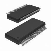
IC 18BIT D F-F 3-ST 56SSOP
Manufacturer
NXP Semiconductors
Series
74ALVCHr
Type
D-Type Busr
Datasheet
1.74ALVCH16823DGG11.pdf
(12 pages)
Specifications of 74ALVCH16823DL,512
Function
Master Reset
Output Type
Tri-State Non Inverted
Number Of Elements
2
Number Of Bits Per Element
9
Frequency - Clock
300MHz
Delay Time - Propagation
2.8ns
Trigger Type
Positive Edge
Current - Output High, Low
24mA, 24mA
Voltage - Supply
2.3 V ~ 2.7 V
Operating Temperature
-40°C ~ 85°C
Mounting Type
Surface Mount
Package / Case
56-SSOP
Lead Free Status / RoHS Status
Lead free / RoHS Compliant
Other names
74ALVCH16823DL
74ALVCH16823DL
935259020512
74ALVCH16823DL
935259020512


1. The input and output voltage ratings may be exceeded if the input and output current ratings are observed.
Philips Semiconductors
FUNCTION TABLE
H = HIGH voltage level
h = HIGH voltage level one set-up time prior to the Low-to-High clock transition
L = LOW voltage level
l
X = Don’t care
Z = HIGH impedance “off” state
RECOMMENDED OPERATING CONDITIONS
ABSOLUTE MAXIMUM RATINGS
In accordance with the Absolute Maximum Rating System (IEC 134). Voltages are referenced to GND (ground = 0V).
NOTE:
1998 Jul 29
SYMBOL
SYMBOL
18-bit D-type flip-flop (3-State)
= LOW voltage level one set-up time prior to the Low-to-High clock transition
= LOW to High clock transition
SYMBOL
I
GND
nOE
T
V
V
V
t
P
H
V
L
L
L
L
L
amb
r
V
V
V
T
I
CC
CC
CC
, t
V
I
TOT
O
V
V
OK
I
CC
IK
stg
I
O
O
, I
f
I
I
CC
DC supply voltage 2.5V range (for max. speed
performance @ 30 pF output load)
DC supply voltage 3.3V range (for max. speed
performance @ 50 pF output load)
DC supply voltage (for low-voltage applications)
DC Input voltage range
DC Input voltage range
DC output voltage range
Operating free-air temperature range
Input rise and fall times
nMR
DC supply voltage
DC input diode current
DC input voltage
DC in ut voltage
DC output diode current
DC output voltage
DC output source or sink current
DC V
Storage temperature range
Power dissipation per package
–plastic medium-shrink (SSOP)
–plastic thin-medium-shrink (TSSOP)
H
H
H
H
L
X
CC
or GND current
PARAMETER
INPUTS
nCE
PARAMETER
PARAMETER
X
H
X
L
L
L
nCP
X
L
X
X
V
For control pins
For data inputs
V
Note 1
V
For temperature range: –40 to +125 C
above +55 C derate linearly with 11.3 mW/K
above +55 C derate linearly with 8 mW/K
I
O
O
t0
nDx
uV
= 0 to V
X
X
X
X
h
l
CC
or V
CC
5
for data input pins
V
V
O
1
for control pins
CC
CC
1
CONDITIONS
CONDITIONS
CONDITIONS
t 0
= 2.3 to 3.0V
= 3.0 to 3.6V
OUTPUT
nQx
Q
Q
H
L
L
Z
0
0
Clear
Load and read data
Load and read data
Hold
Hold
Disable outputs
MIN
–40
2.3
3.0
1.2
0
0
0
0
0
OPERATING MODES
OPERATING MODES
LIMITS
–0.5 to V
–0.5 to V
–0.5 to +4.6
–0.5 to +5.5
–65 to +150
74ALVCH16823
RATING
"100
"50
"50
–50
850
600
MAX
V
V
+85
2.7
3.6
3.6
5.5
CC
CC
20
10
CC
CC
+0.5
+0.5
Product specification
UNIT
UNIT
ns/V
UNIT
mW
mA
mA
mA
mA
V
V
V
V
V
V
C
V
V
V
V
C
Related parts for 74ALVCH16823DL,512
Image
Part Number
Description
Manufacturer
Datasheet
Request
R

Part Number:
Description:
NXP Semiconductors designed the LPC2420/2460 microcontroller around a 16-bit/32-bitARM7TDMI-S CPU core with real-time debug interfaces that include both JTAG andembedded trace
Manufacturer:
NXP Semiconductors
Datasheet:

Part Number:
Description:
NXP Semiconductors designed the LPC2458 microcontroller around a 16-bit/32-bitARM7TDMI-S CPU core with real-time debug interfaces that include both JTAG andembedded trace
Manufacturer:
NXP Semiconductors
Datasheet:
Part Number:
Description:
NXP Semiconductors designed the LPC2468 microcontroller around a 16-bit/32-bitARM7TDMI-S CPU core with real-time debug interfaces that include both JTAG andembedded trace
Manufacturer:
NXP Semiconductors
Datasheet:
Part Number:
Description:
NXP Semiconductors designed the LPC2470 microcontroller, powered by theARM7TDMI-S core, to be a highly integrated microcontroller for a wide range ofapplications that require advanced communications and high quality graphic displays
Manufacturer:
NXP Semiconductors
Datasheet:
Part Number:
Description:
NXP Semiconductors designed the LPC2478 microcontroller, powered by theARM7TDMI-S core, to be a highly integrated microcontroller for a wide range ofapplications that require advanced communications and high quality graphic displays
Manufacturer:
NXP Semiconductors
Datasheet:
Part Number:
Description:
The Philips Semiconductors XA (eXtended Architecture) family of 16-bit single-chip microcontrollers is powerful enough to easily handle the requirements of high performance embedded applications, yet inexpensive enough to compete in the market for hi
Manufacturer:
NXP Semiconductors
Datasheet:
Part Number:
Description:
The XA-S3 device is a member of Philips Semiconductors? XA(eXtended Architecture) family of high performance 16-bitsingle-chip microcontrollers
Manufacturer:
NXP Semiconductors
Datasheet:

Part Number:
Description:
The NXP BlueStreak LH75401/LH75411 family consists of two low-cost 16/32-bit System-on-Chip (SoC) devices
Manufacturer:
NXP Semiconductors
Datasheet:
Part Number:
Description:
The NXP LPC3130/3131 combine an 180 MHz ARM926EJ-S CPU core, high-speed USB2
Manufacturer:
NXP Semiconductors
Datasheet:
Part Number:
Description:
The NXP LPC3141 combine a 270 MHz ARM926EJ-S CPU core, High-speed USB 2
Manufacturer:
NXP Semiconductors
Part Number:
Description:
The NXP LPC3143 combine a 270 MHz ARM926EJ-S CPU core, High-speed USB 2
Manufacturer:
NXP Semiconductors

Part Number:
Description:
The NXP LPC3152 combines an 180 MHz ARM926EJ-S CPU core, High-speed USB 2
Manufacturer:
NXP Semiconductors
Part Number:
Description:
The NXP LPC3154 combines an 180 MHz ARM926EJ-S CPU core, High-speed USB 2
Manufacturer:
NXP Semiconductors

Part Number:
Description:
Standard level N-channel enhancement mode Field-Effect Transistor (FET) in a plastic package using NXP High-Performance Automotive (HPA) TrenchMOS technology
Manufacturer:
NXP Semiconductors
Datasheet: