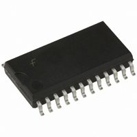
74F825SC Fairchild Semiconductor, 74F825SC Datasheet - Page 2

74F825SC
Manufacturer Part Number
74F825SC
Description
IC F/F DUAL D-TYPE 8BIT 24-SOIC
Manufacturer
Fairchild Semiconductor
Series
74Fr
Type
D-Type Busr
Datasheet
1.74F825SPC.pdf
(6 pages)
Specifications of 74F825SC
Function
Master Reset
Output Type
Tri-State Non Inverted
Number Of Elements
1
Number Of Bits Per Element
8
Frequency - Clock
160MHz
Delay Time - Propagation
6.5ns
Trigger Type
Positive Edge
Current - Output High, Low
3mA, 24mA
Voltage - Supply
4.5 V ~ 5.5 V
Operating Temperature
0°C ~ 70°C
Mounting Type
Surface Mount
Package / Case
24-SOIC (7.5mm Width)
Lead Free Status / RoHS Status
Lead free / RoHS Compliant
www.fairchildsemi.com
Unit Loading/Fan Out
Functional Description
The 74F825 consists of eight D-type edge-triggered
flip-flops. This device has 3-STATE true outputs and is
organized in broadside pinning. In addition to the clock and
output enable pins, the buffered clock (CP) and buffered
Output Enable (OE) are common to all flip-flops. The
flip-flops will store the state of their individual D inputs that
meet the setup and hold times requirements on the
LOW-to-HIGH CP transition. With the OE LOW the con-
tents of the flip-flops are available at the outputs. When the
OE is HIGH, the outputs go to the high impedance state.
Operation of the OE input does not affect the state of the
flip-flops. The 74F825 has Clear (CLR) and Clock Enable
(EN) pins.
When the CLR is LOW and the OE is LOW the outputs are
LOW. When CLR is HIGH, data can be entered into the
flip-flops. When EN is LOW, data on the inputs is trans-
ferred to the outputs on the LOW-to-HIGH clock transition.
When the EN is HIGH the outputs do not change state,
regardless of the data or clock input transitions.
Logic Diagram
Please note that this diagram is provided only for the understanding of logic operations and should not be used to estimate propagation delays.
D
O
OE
EN
CLR
CP
0
0
–D
–O
1
, OE
Pin Names
7
7
2
, OE
3
Data Inputs
3-STATE Data Outputs
Output Enable Input
Clock Enable
Clear
Clock Input
Description
2
Function Table
OE CLR EN CP D
L
H
X
H
H
H
H
H
H
L
L
L
L
L
L
LOW Voltage Level
HIGH Voltage Level
Immaterial
150/40 (33.3)
HIGH/LOW
H
H
H
H
H
H
H
H
H
H
1.0/1.0
1.0/1.0
1.0/1.0
1.0/1.0
1.0/2.0
L
L
Inputs
U.L.
L
L
H
H
X
X
L
L
L
L
L
L
H X
H X
L
X
X
X
X
L
H
H
X
X
X
X
X
X
L
L
Internal Output
3 mA/24 mA (20 mA)
NC
NC
NC
NC
NC
NC
Q
H
H
H
H
Output I
20 A/ 0.6 mA
20 A/ 0.6 mA
20 A/ 0.6 mA
20 A/ 0.6 mA
20 A/ 1.2 mA
L
L
NC
Input I
Z
High Impedance
LOW-to-HIGH Transition
No Change
NC
NC
NC
IH
OH
O
H
Z
Z
Z
Z
L
Z
Z
L
/I
/I
IL
OL
Hold
Hold
Hold
Hold
Clear
Clear
Load
Load
Data Available
Data Available
No Change in Data
No Change in Data
Function


