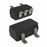
74AHC1GU04GW,125 NXP Semiconductors, 74AHC1GU04GW,125 Datasheet - Page 5

74AHC1GU04GW,125
Manufacturer Part Number
74AHC1GU04GW,125
Description
IC INVERTER 5-TSSOP
Manufacturer
NXP Semiconductors
Series
74AHCr
Datasheet
1.74AHC1GU04GW125.pdf
(12 pages)
Specifications of 74AHC1GU04GW,125
Number Of Circuits
1
Logic Type
Inverter
Package / Case
SC-70-5, SC-88A, SOT-323-5, SOT-353, 5-TSSOP
Number Of Inputs
1
Current - Output High, Low
8mA, 8mA
Voltage - Supply
2 V ~ 5.5 V
Operating Temperature
-40°C ~ 125°C
Mounting Type
Surface Mount
Logic Family
AHC
High Level Output Current
- 8 mA
Low Level Output Current
8 mA
Supply Voltage (max)
5.5 V
Supply Voltage (min)
2 V
Maximum Operating Temperature
+ 125 C
Mounting Style
SMD/SMT
Operating Supply Voltage
5 V
Lead Free Status / RoHS Status
Lead free / RoHS Compliant
Lead Free Status / RoHS Status
Lead free / RoHS Compliant, Lead free / RoHS Compliant
Other names
568-4825-2
74AHC1GU04GW,125
74AHC1GU04GW-G
74AHC1GU04GW-G
935263016125
74AHC1GU04GW,125
74AHC1GU04GW-G
74AHC1GU04GW-G
935263016125
NXP Semiconductors
12. Waveforms
13. Typical transfer characteristics
74AHC1GU04_5
Product data sheet
Fig 5. The input (A) to output (Y) propagation delay
Fig 7. V
f
C
V
o
V
(V)
CC
L
= output frequency in MHz;
O
= output load capacitance in pF;
2.0
1.6
1.2
0.8
0.4
= supply voltage in Volts.
Y output
0
A input
V
times
0
M
CC
= 0.5
= 2.0 V; I
0.4
V
V
CC
O
; V
O
V
M
= 0 A
I
0.8
(1)
V
= GND to V
M
(1)
t
PHL
1.2
I
D
CC
(drain current)
.
1.6
V
mna397
I
(V)
t
PLH
mna046
2.0
Rev. 05 — 10 July 2007
1.0
0.8
0.6
0.4
0.2
0
(mA)
I
CC
Fig 6. Load circuitry for switching times
Fig 8. V
V
(V)
3.0
1.5
O
0
GENERATOR
Test data is given in
Definitions for test circuit:
C
capacitance.
R
output impedance Z
0
L
T
CC
PULSE
= Load capacitance including jig and probe
= Termination resistance should be equal to
= 3.0 V; I
V
O
O
V I
1
= 0 A
o
Table
of the pulse generator.
74AHC1GU04
R T
8.
DUT
V
CC
I
D
2
(drain current)
© NXP B.V. 2007. All rights reserved.
V O
V
I
(V)
mna398
mna034
C L
50 pF
3
10
8
6
4
2
0
Inverter
(mA)
I
CC
5 of 12


