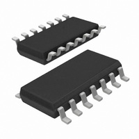
74HCU04D,653 NXP Semiconductors, 74HCU04D,653 Datasheet - Page 7

74HCU04D,653
Manufacturer Part Number
74HCU04D,653
Description
IC INVERTER HEX UNBUFFER 14SOIC
Manufacturer
NXP Semiconductors
Series
74HCUr
Datasheet
1.74HCU04D653.pdf
(7 pages)
Specifications of 74HCU04D,653
Number Of Circuits
6
Logic Type
Inverter
Package / Case
14-SOIC (3.9mm Width), 14-SOL
Number Of Inputs
1
Current - Output High, Low
5.2mA, 5.2mA
Voltage - Supply
2 V ~ 6 V
Operating Temperature
-40°C ~ 125°C
Mounting Type
Surface Mount
Logic Family
74HCU
High Level Output Current
- 5.2 mA
Low Level Output Current
5.2 mA
Propagation Delay Time
70 ns, 14 ns, 12 ns
Supply Voltage (max)
6 V
Supply Voltage (min)
2 V
Maximum Operating Temperature
+ 125 C
Minimum Operating Temperature
- 40 C
Mounting Style
SMD/SMT
Operating Supply Voltage
2 V to 6 V
Lead Free Status / RoHS Status
Lead free / RoHS Compliant
Lead Free Status / RoHS Status
Lead free / RoHS Compliant, Lead free / RoHS Compliant
Other names
568-1571-2
74HCU04D-T
933714000653
74HCU04D-T
933714000653
Philips Semiconductors
OPTIMUM VALUE FOR R
EXTERNAL COMPONENTS FOR RESONATOR
(f
Note
1. All values given are typical and must be used as an
September 1993
130 to 199.9
200 to 349.9
350 to 600
FREQUENCY
FREQUENCY
C
C
R
R
stability against changes in V
(I
10 to 15.9
16 to 24.9
25 to 54.9
55 to 129.9
Hex inverter
CC
1
2
1
2
1 MHz)
initial set-up.
= 47 pF (typ.)
= 33 pF (typ.)
= 1 to 10 M (typ.)
optimum value depends on the frequency and required
is typically 5 mA at V
(MHz)
10
14
14
(kHz)
3
6
Fig.13 Crystal oscillator configuration.
2
8
1
4.7
0.5
2
0.5
1
(k )
R
replace R
value of 35 pF
(M )
CC
2
R
22
22
22
22
22
10
10
= 5 V and f = 10 MHz).
1
CC
minimum required I
minimum influence due to
change in V
minimum I
minimum influence by V
minimum I
minimum influence by V
minimum I
minimum influence by V
or average minimum I
2
2
by C
(k )
OPTIMUM FOR
220
220
100
100
R
47
47
47
2
CC
CC
CC
3
CC
with a typical
CC
(pF)
C
CC
1
56
56
56
47
47
47
47
CC
CC
CC
(pF)
C
2
20
10
10
5
5
5
5
7
Note to Application information
All values given are typical unless otherwise specified.
PACKAGE OUTLINES
See
R
The average I
3.5 + 0.05
(for more information refer to “DESIGNERS GUIDE” ).
S
f
(1) V
(2) V
(3) V
(4) V
(5) V
Fig.15 Typical input capacitance as a function of
“74HC/HCT/HCU/HCMOS Logic Package Outlines”
=
Fig.14 HCU04 used as an astable multivibrator
2 R.
1
-- -
T
CC
CC
CC
CC
CC
----------------- -
2.2 RC
= 2.0 V.
= 3.0 V.
= 4.0 V.
= 5.0 V.
= 6.0 V.
f (MHz) C (pF) at V
input voltage.
1
CC
(mA) is approximately
CC
= 5.0 V
Product specification
74HCU04
.


