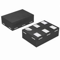
74LVC1G14GM,115 NXP Semiconductors, 74LVC1G14GM,115 Datasheet - Page 6

74LVC1G14GM,115
Manufacturer Part Number
74LVC1G14GM,115
Description
IC SNGL SCHMITT TRIG INV 6-XSON
Manufacturer
NXP Semiconductors
Series
74LVCr
Datasheet
1.74LVC1G14GV125.pdf
(19 pages)
Specifications of 74LVC1G14GM,115
Number Of Circuits
1
Logic Type
Inverter with Schmitt Trigger
Package / Case
6-XSON (Micropak™), SOT-886
Number Of Inputs
1
Current - Output High, Low
32mA, 32mA
Voltage - Supply
1.65 V ~ 5.5 V
Operating Temperature
-40°C ~ 125°C
Mounting Type
Surface Mount
Logic Family
74LVC
High Level Output Current
- 32 mA
Low Level Output Current
32 mA
Supply Voltage (max)
5.5 V
Supply Voltage (min)
1.65 V
Maximum Operating Temperature
+ 125 C
Minimum Operating Temperature
- 40 C
Mounting Style
SMD/SMT
Operating Supply Voltage
1.8 V, 2.5 V, 3.3 V, 5 V
Lead Free Status / RoHS Status
Lead free / RoHS Compliant
Lead Free Status / RoHS Status
Lead free / RoHS Compliant, Lead free / RoHS Compliant
Other names
568-4397-2
74LVC1G14GM-G
74LVC1G14GM-G
935277179115
74LVC1G14GM-G
74LVC1G14GM-G
935277179115
NXP Semiconductors
Table 8.
Voltages are referenced to GND (ground = 0 V); for load circuit see
[1]
12. Dynamic characteristics
Table 9.
Voltages are referenced to GND (ground = 0 V); for load circuit see
[1]
[2]
[3]
74LVC1G14
Product data sheet
Symbol Parameter
V
V
Symbol Parameter
t
C
pd
T−
H
PD
All typical values are measured at T
Typical values are measured at T
t
C
P
f
f
C
V
pd
i
o
D
CC
PD
= input frequency in MHz;
L
= output frequency in MHz;
is the same as t
= output load capacitance in pF;
= C
is used to determine the dynamic power dissipation (P
= supply voltage in V.
propagation delay A to Y; see
power dissipation
capacitance
negative-going
threshold voltage
hysteresis voltage (V
PD
Transfer characteristics
Dynamic characteristics
× V
CC
2
× f
PLH
i
+ (C
and t
L
× V
PHL
Conditions
see
Figure 10
Conditions
V
CC
CC
.
V
V
V
V
V
T+
V
V
V
V
V
V
V
V
V
V
2
amb
CC
CC
CC
CC
CC
CC
CC
CC
CC
CC
CC
CC
CC
CC
CC
× f
Figure 9
= 3.3 V; V
− V
amb
o
= 1.8 V
= 2.3 V
= 3.0 V
= 4.5 V
= 5.5 V
= 1.8 V
= 2.3 V
= 3.0 V
= 4.5 V
= 5.5 V
= 1.65 V to 1.95 V
= 2.3 V to 2.7 V
= 2.7 V
= 3.0 V to 3.6 V
= 4.5 V to 5.5 V
= 25 °C and V
) where:
…continued
T−
= 25 °C
and
); see
Figure 7
All information provided in this document is subject to legal disclaimers.
and
Figure 11
I
= GND to V
Figure
Figure 10
Rev. 8 — 10 November 2010
CC
= 1.8 V, 2.5 V, 2.7 V, 3.3 V and 5.0 V respectively.
9,
D
CC
in μW).
[2]
[3]
0.46
0.65
0.88
1.32
1.58
0.26
0.28
0.31
0.40
0.47
Min
Figure
Figure
Min
1.0
0.7
0.7
0.7
0.7
−40 °C to +85 °C
-
−40 °C to +85 °C
8.
8.
Typ
Typ
0.6
0.8
1.0
1.5
1.8
0.4
0.4
0.5
0.6
0.6
15.4
4.1
2.8
3.2
3.0
2.2
[1]
[1]
Max
0.75
0.96
1.24
1.84
2.24
0.51
0.57
0.64
0.77
0.88
Max
11.0
6.5
6.5
5.5
5.0
Single Schmitt-trigger inverter
-
−40 °C to +125 °C Unit
−40 °C to +125 °C
74LVC1G14
0.46
0.65
0.88
1.32
1.58
0.19
0.22
0.25
0.34
0.41
Min
Min
1.0
0.7
0.7
0.7
0.7
-
© NXP B.V. 2010. All rights reserved.
Max
14.0
8.5
8.5
7.0
6.5
0.78
0.99
1.27
1.87
2.27
0.51
0.57
0.64
0.77
0.88
Max
-
ns
ns
ns
ns
ns
pF
Unit
V
V
V
V
V
V
V
V
V
V
6 of 19


