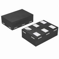
74AUP1G240GM,115 NXP Semiconductors, 74AUP1G240GM,115 Datasheet - Page 2

74AUP1G240GM,115
Manufacturer Part Number
74AUP1G240GM,115
Description
IC INVERTER 1-INPUT 6XSON
Manufacturer
NXP Semiconductors
Series
74AUPr
Datasheet
1.74AUP1G240GM115.pdf
(22 pages)
Specifications of 74AUP1G240GM,115
Package / Case
6-XSON (Micropak™), SOT-886
Logic Type
Inverter
Number Of Inputs
1
Number Of Circuits
1
Current - Output High, Low
4mA, 4mA
Voltage - Supply
0.8 V ~ 3.6 V
Operating Temperature
-40°C ~ 125°C
Mounting Type
Surface Mount
Logic Family
AUP
Number Of Channels Per Chip
1
Polarity
Inverting
Supply Voltage (max)
3.6 V
Supply Voltage (min)
0.8 V
Maximum Operating Temperature
+ 125 C
Mounting Style
SMD/SMT
High Level Output Current
- 4 mA
Input Bias Current (max)
0.5 uA
Low Level Output Current
4 mA
Minimum Operating Temperature
- 40 C
Output Type
3-State
Propagation Delay Time
21.6 ns @ 1.1 V to 1.3 V or 12.3 ns @ 1.4 V to 1.6 V or 9.5 ns @ 1.65 V to 1.95 V or 7.1 ns @ 2.3 V to 2.7 V or 6.4 ns @ 3 V to 3.6 V
Number Of Lines (input / Output)
1 / 1
Lead Free Status / RoHS Status
Lead free / RoHS Compliant
Lead Free Status / RoHS Status
Lead free / RoHS Compliant, Lead free / RoHS Compliant
Other names
568-4379-2
74AUP1G240GM-G
74AUP1G240GM-G
935279062115
74AUP1G240GM-G
74AUP1G240GM-G
935279062115
NXP Semiconductors
3. Ordering information
Table 1.
4. Marking
Table 2.
[1]
5. Functional diagram
74AUP1G240
Product data sheet
Type number
74AUP1G240GW
74AUP1G240GM
74AUP1G240GF
74AUP1G240GN
74AUP1G240GS
Type number
74AUP1G240GW
74AUP1G240GM
74AUP1G240GF
74AUP1G240GN
74AUP1G240GS
Fig 1.
The pin 1 indicator is located on the lower left corner of the device, below the marking code.
Logic symbol
2
1
Ordering information
Marking
A
OE
001aac528
Package
Temperature range Name
−40 °C to +125 °C
−40 °C to +125 °C
−40 °C to +125 °C
−40 °C to +125 °C
−40 °C to +125 °C
Y
4
All information provided in this document is subject to legal disclaimers.
Fig 2.
TSSOP5
XSON6
XSON6
XSON6
XSON6
Rev. 2 — 13 September 2010
IEC logic symbol
2
1
OE
Description
plastic thin shrink small outline package; 5 leads;
body width 1.25 mm
plastic extremely thin small outline package; no leads;
6 terminals; body 1 × 1.45 × 0.5 mm
plastic extremely thin small outline package; no leads;
6 terminals; body 1 × 1 × 0.5 mm
extremely thin small outline package; no leads;
6 terminals; body 0.9 × 1.0 × 0.35 mm
extremely thin small outline package; no leads;
6 terminals; body 1.0 × 1.0 × 0.35 mm
001aac527
Marking code
p2
p2
p2
p2
p2
Low-power inverting buffer/line driver; 3-state
4
[1]
Fig 3.
OE
A
74AUP1G240
Logic diagram
© NXP B.V. 2010. All rights reserved.
001aac526
Version
SOT353-1
SOT886
SOT891
SOT1115
SOT1202
Y
2 of 22


