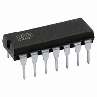
74HCT04N,652 NXP Semiconductors, 74HCT04N,652 Datasheet - Page 2

74HCT04N,652
Manufacturer Part Number
74HCT04N,652
Description
IC INVERTER HEX TTL/LSTTL 14DIP
Manufacturer
NXP Semiconductors
Series
74HCTr
Datasheet
1.74HC04BQ115.pdf
(20 pages)
Specifications of 74HCT04N,652
Number Of Circuits
6
Logic Type
Inverter
Package / Case
14-DIP (0.300", 7.62mm)
Number Of Inputs
1
Current - Output High, Low
4mA, 4mA
Voltage - Supply
4.5 V ~ 5.5 V
Operating Temperature
-40°C ~ 125°C
Mounting Type
Through Hole
Logic Family
74HCT
High Level Output Current
- 4 mA
Low Level Output Current
4 mA
Propagation Delay Time
8 ns
Supply Voltage (max)
5.5 V
Supply Voltage (min)
4.5 V
Maximum Operating Temperature
+ 125 C
Minimum Operating Temperature
- 40 C
Mounting Style
Through Hole
Operating Supply Voltage
4.5 V to 5.5 V
Logical Function
Inverter
Number Of Elements
6
Operating Supply Voltage (typ)
5V
Package Type
DIP
Operating Temp Range
-40C to 125C
Pin Count
14
Quiescent Current
2uA
Technology
CMOS
Mounting
Through Hole
Operating Temperature Classification
Automotive
Operating Supply Voltage (max)
5.5V
Operating Supply Voltage (min)
4.5V
Lead Free Status / RoHS Status
Lead free / RoHS Compliant
Lead Free Status / RoHS Status
Lead free / RoHS Compliant, Lead free / RoHS Compliant
Other names
568-1503-5
74HCT04N
933668900652
74HCT04N
933668900652
Philips Semiconductors
FEATURES
QUICK REFERENCE DATA
GND = 0 V; T
Notes
1. C
2. For 74HC04: the condition is V
FUNCTION TABLE
See note 1.
Note
1. H = HIGH voltage level;
2003 Jul 23
t
C
C
SYMBOL
PHL
Complies with JEDEC standard no. 8-1A
ESD protection:
HBM EIA/JESD22-A114-A exceeds 2000 V
MM EIA/JESD22-A115-A exceeds 200 V.
Specified from 40 to +85 C and 40 to +125 C.
I
PD
Hex inverter
P
f
f
C
V
N = total load switching outputs;
For 74HCT04: the condition is V
L = LOW voltage level.
i
o
/t
(C
D
CC
PD
= input frequency in MHz;
L
PLH
= output frequency in MHz;
= output load capacitance in pF;
= C
L
is used to determine the dynamic power dissipation (P
= supply voltage in Volts;
PD
V
CC
propagation delay nA to nY
input capacitance
power dissipation capacitance per gate notes 1 and 2
amb
2
V
CC
= 25 C; t
f
o
2
) = sum of the outputs.
f
i
PARAMETER
INPUT
N + (C
r
= t
nA
H
L
f
6.0 ns.
L
I
= GND to V
I
= GND to V
V
CC
2
f
o
) where:
CC
CC
.
C
1.5 V.
L
= 15 pF; V
2
CONDITIONS
DESCRIPTION
The 74HC/HCT04 are high-speed Si-gate CMOS devices
and are pin compatible with low power Schottky TTL
(LSTTL). They are specified in compliance with JEDEC
standard no. 7A. The 74HC/HCT04 provide six inverting
buffers.
D
in W).
CC
= 5 V
7
3.5
21
OUTPUT
HC04
74HC04; 74HCT04
nY
H
L
TYPICAL
8
3.5
24
Product specification
HCT04
ns
pF
pF
UNIT


