N74F3038D,518 NXP Semiconductors, N74F3038D,518 Datasheet - Page 4
N74F3038D,518
Manufacturer Part Number
N74F3038D,518
Description
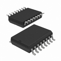
IC GATE NAND QUAD 2INPUT 16SOICW
Manufacturer
NXP Semiconductors
Series
74Fr
Datasheet
1.N74F3038DG518.pdf
(8 pages)
Specifications of N74F3038D,518
Number Of Circuits
4
Package / Case
16-SOIC (0.300", 7.5mm Width)
Logic Type
NAND Gate
Number Of Inputs
2
Voltage - Supply
4.5 V ~ 5.5 V
Operating Temperature
0°C ~ 70°C
Mounting Type
Surface Mount
Logic Family
F
High Level Output Current
- 0.25 mA
Low Level Output Current
160 mA
Propagation Delay Time
11.5 ns
Supply Voltage (max)
5.5 V
Supply Voltage (min)
4.5 V
Maximum Operating Temperature
+ 70 C
Mounting Style
SMD/SMT
Minimum Operating Temperature
0 C
Lead Free Status / RoHS Status
Lead free / RoHS Compliant
Current - Output High, Low
-
Lead Free Status / Rohs Status
Lead free / RoHS Compliant
Other names
935008190518
N74F3038D-T
N74F3038D-T
N74F3038D-T
N74F3038D-T


1. For conditions shown as MIN or MAX, use the appropriate value specified under recommended operating conditions for the applicable type.
2. All typical values are at V
3. I
Philips Semiconductors
DC ELECTRICAL CHARACTERISTICS
(Over recommended operating free-air temperature range unless otherwise noted.)
NOTES:
AC ELECTRICAL CHARACTERISTICS
AC WAVEFORMS
For all waveforms, V
1998 May 21
SYMBOL
SYMBOL
SYMBOL
t
t
PLH
PHL
Quad 2-input NAND 30 line driver (open collector)
V
V
OL1
I
Dna, Dnb
V
I
I
I
OH
I
CC
CC
Waveform 1.
I
IH
O
OL
IL
IK
I
is the current necessary to guarantee the High to Low transition in a 30 transmission line on the incident wave.
Qn
High-level output current
Low level output current
Low-level output current
Input clamp voltage
Input current at maximum input
voltage
High-level input current
Low-level input current
Supply current (total)
Supply current (total)
Propagation delay
Dna, Dnb to Qn
M
Propagation Delay for Inputs to Output
= 1.5V.
PARAMETER
PARAMETER
V
PARAMETER
M
CC
t
PHL
V
= 5V, T
M
V
amb
M
I
I
CCH
CCL
= 25 C.
t
PLH
V
V
V
V
V
M
CC
V
CC
IL
IL
IH
= MIN, V
= MAX
= MAX
= MIN
= MIN
CONDITION
V
V
Waveform 1
SF00005
CC
CC
V
V
V
TEST
TEST CONDITIONS
TEST CONDITIONS
IL
CC
CC
CC
= MAX
= MAX
V
= MAX, V
CC
I
I
OL
= MAX, V
= MAX, V
= MAX, V
OL
= MIN, I
= 160mA
= 100mA
4
IH
I
I
I
I
= MIN, V
= 7.0V
= 2.7V
= 0.5V
= I
C
MIN
6.0
1.0
3
L
IK
= 50pF, R
T
1
1
V
amb
V
CC
V
10% V
IN
IN
OH
5% V
TYP
= +5.0V
8.5
2.0
= +25 C
= GND
= 4.5V
= MAX
L
CC
CC
= 500
MAX
11.5
5.0
LIMITS
MIN
C
T
V
L
amb
MIN
CC
6.0
1.0
= 50pF, R
= +5.0V
= 0 C to +70 C
LIMITS
–0.73
TYP
0.42
3.5
30
2
L
= 500
MAX
12.0
10%
5.0
Product specification
74F3038
MAX
0.55
0.80
–1.2
–0.6
250
100
6.0
20
40
UNIT
ns
UNIT
UNIT
mA
mA
mA
V
V
V
A
A
A
Related parts for N74F3038D,518
Image
Part Number
Description
Manufacturer
Datasheet
Request
R

Part Number:
Description:
NXP Semiconductors designed the LPC2420/2460 microcontroller around a 16-bit/32-bitARM7TDMI-S CPU core with real-time debug interfaces that include both JTAG andembedded trace
Manufacturer:
NXP Semiconductors
Datasheet:

Part Number:
Description:
NXP Semiconductors designed the LPC2458 microcontroller around a 16-bit/32-bitARM7TDMI-S CPU core with real-time debug interfaces that include both JTAG andembedded trace
Manufacturer:
NXP Semiconductors
Datasheet:
Part Number:
Description:
NXP Semiconductors designed the LPC2468 microcontroller around a 16-bit/32-bitARM7TDMI-S CPU core with real-time debug interfaces that include both JTAG andembedded trace
Manufacturer:
NXP Semiconductors
Datasheet:
Part Number:
Description:
NXP Semiconductors designed the LPC2470 microcontroller, powered by theARM7TDMI-S core, to be a highly integrated microcontroller for a wide range ofapplications that require advanced communications and high quality graphic displays
Manufacturer:
NXP Semiconductors
Datasheet:
Part Number:
Description:
NXP Semiconductors designed the LPC2478 microcontroller, powered by theARM7TDMI-S core, to be a highly integrated microcontroller for a wide range ofapplications that require advanced communications and high quality graphic displays
Manufacturer:
NXP Semiconductors
Datasheet:
Part Number:
Description:
The Philips Semiconductors XA (eXtended Architecture) family of 16-bit single-chip microcontrollers is powerful enough to easily handle the requirements of high performance embedded applications, yet inexpensive enough to compete in the market for hi
Manufacturer:
NXP Semiconductors
Datasheet:
Part Number:
Description:
The XA-S3 device is a member of Philips Semiconductors? XA(eXtended Architecture) family of high performance 16-bitsingle-chip microcontrollers
Manufacturer:
NXP Semiconductors
Datasheet:

Part Number:
Description:
The NXP BlueStreak LH75401/LH75411 family consists of two low-cost 16/32-bit System-on-Chip (SoC) devices
Manufacturer:
NXP Semiconductors
Datasheet:
Part Number:
Description:
The NXP LPC3130/3131 combine an 180 MHz ARM926EJ-S CPU core, high-speed USB2
Manufacturer:
NXP Semiconductors
Datasheet:
Part Number:
Description:
The NXP LPC3141 combine a 270 MHz ARM926EJ-S CPU core, High-speed USB 2
Manufacturer:
NXP Semiconductors
Part Number:
Description:
The NXP LPC3143 combine a 270 MHz ARM926EJ-S CPU core, High-speed USB 2
Manufacturer:
NXP Semiconductors

Part Number:
Description:
The NXP LPC3152 combines an 180 MHz ARM926EJ-S CPU core, High-speed USB 2
Manufacturer:
NXP Semiconductors
Part Number:
Description:
The NXP LPC3154 combines an 180 MHz ARM926EJ-S CPU core, High-speed USB 2
Manufacturer:
NXP Semiconductors

Part Number:
Description:
Standard level N-channel enhancement mode Field-Effect Transistor (FET) in a plastic package using NXP High-Performance Automotive (HPA) TrenchMOS technology
Manufacturer:
NXP Semiconductors
Datasheet: