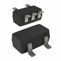
74LVC1G32GW,125 NXP Semiconductors, 74LVC1G32GW,125 Datasheet - Page 5

74LVC1G32GW,125
Manufacturer Part Number
74LVC1G32GW,125
Description
IC SNGL 2-IN POS-OR GATE SOT-353
Manufacturer
NXP Semiconductors
Series
74LVCr
Datasheet
1.74LVC1G32GV125.pdf
(17 pages)
Specifications of 74LVC1G32GW,125
Number Of Circuits
1
Package / Case
SC-70-5, SC-88A, SOT-323-5, SOT-353, 5-TSSOP
Logic Type
OR Gate
Number Of Inputs
2
Current - Output High, Low
32mA, 32mA
Voltage - Supply
1.65 V ~ 5.5 V
Operating Temperature
-40°C ~ 125°C
Mounting Type
Surface Mount
Product
OR
Logic Family
74LVC
High Level Output Current
- 32 mA
Low Level Output Current
32 mA
Propagation Delay Time
5.5 ns
Supply Voltage (max)
5.5 V
Supply Voltage (min)
1.65 V
Maximum Operating Temperature
+ 125 C
Mounting Style
SMD/SMT
Minimum Operating Temperature
- 40 C
Logical Function
OR
Number Of Elements
1
Operating Supply Voltage (typ)
1.8/2.5/3.3/5V
Operating Temp Range
-40C to 125C
Package Type
TSSOP
Number Of Outputs
1
Technology
CMOS
Mounting
Surface Mount
Pin Count
5
Operating Temperature Classification
Automotive
Operating Supply Voltage (max)
5.5V
Operating Supply Voltage (min)
1.65V
Lead Free Status / RoHS Status
Lead free / RoHS Compliant
Lead Free Status / RoHS Status
Lead free / RoHS Compliant, Lead free / RoHS Compliant
Other names
568-2298-2
74LVC1G32GW-G
935268381125
74LVC1G32GW-G
935268381125
Available stocks
Company
Part Number
Manufacturer
Quantity
Price
Company:
Part Number:
74LVC1G32GW,125
Manufacturer:
NXP Semiconductors
Quantity:
4 000
NXP Semiconductors
10. Static characteristics
Table 7.
At recommended operating conditions. Voltages are referenced to GND (ground = 0 V).
[1]
74LVC1G32
Product data sheet
Symbol Parameter
V
V
V
V
I
I
I
ΔI
C
I
OFF
CC
IH
IL
OH
OL
I
CC
All typical values are measured at V
HIGH-level
input voltage
LOW-level
input voltage
HIGH-level
output voltage
LOW-level
output voltage
input leakage
current
power-off
leakage
current
supply current V
additional
supply current
input
capacitance
Static characteristics
Conditions
V
V
V
V
V
V
V
V
V
V
V
V
V
V
per pin; V
V
V
CC
CC
CC
CC
CC
CC
CC
CC
I
I
I
CC
CC
I
CC
I
CC
I
V
I
I
I
I
I
I
V
I
I
I
I
I
= V
= V
= 5.5 V or GND;
= 5.5 V or GND; I
= V
O
O
O
O
O
O
O
O
O
O
O
O
CC
CC
= 1.65 V to 1.95 V
= 2.3 V to 2.7 V
= 2.7 V to 3.6 V
= 4.5 V to 5.5 V
= 1.65 V to 1.95 V
= 2.3 V to 2.7 V
= 2.7 V to 3.6 V
= 4.5 V to 5.5 V
= 0 V to 5.5 V
= 0 V; V
= 1.65 V to 5.5 V
= 3.3 V; V
= −100 μA;
= −4 mA; V
= −8 mA; V
= −12 mA; V
= −24 mA; V
= −32 mA; V
= 100 μA;
= 4 mA; V
= 8 mA; V
= 12 mA; V
= 24 mA; V
= 32 mA; V
IH
IH
CC
= 1.65 V to 5.5 V
= 1.65 V to 5.5 V
or V
or V
− 0.6 V; I
CC
CC
= 3.3 V and T
IL
IL
I
= 2.3 V to 5.5 V;
or V
I
CC
CC
= GND to V
All information provided in this document is subject to legal disclaimers.
CC
CC
CC
CC
CC
CC
CC
CC
O
= 1.65 V
= 2.3 V
O
= 1.65 V
= 2.3 V
= 2.7 V
= 3.0 V
= 4.5 V
= 5.5 V
O
= 0 A
= 2.7 V
= 3.0 V
= 4.5 V
= 0 A;
Rev. 7 — 20 October 2010
amb
CC
= 25 °C.
V
0.65V
0.7V
CC
Min
1.7
2.0
1.2
1.9
2.2
2.3
3.8
-
-
-
-
-
-
-
-
-
-
-
-
-
-
-
− 0.1
CC
−40 °C to +85 °C
CC
Typ
±0.1
±0.1
0.1
5
5
-
-
-
-
-
-
-
-
-
-
-
-
-
-
-
-
-
-
-
-
[1]
0.35V
0.3V
Max
0.10
0.45
0.30
0.40
0.55
0.55
±10
500
0.7
0.8
±5
10
-
-
-
-
-
-
-
-
-
-
-
CC
CC
V
0.65V
0.7V
−40 °C to +125 °C
CC
74LVC1G32
Single 2-input OR gate
0.95
Min
1.7
2.0
1.7
1.9
2.0
3.4
-
-
-
-
-
-
-
-
-
-
-
-
-
-
-
− 0.1
CC
CC
© NXP B.V. 2010. All rights reserved.
0.35V
0.3V
±100
±200
5000
Max
0.10
0.70
0.45
0.60
0.80
0.80
200
0.7
0.8
-
-
-
-
-
-
-
-
-
-
-
CC
CC
5 of 17
Unit
V
V
V
V
V
V
V
V
V
V
V
V
V
V
V
V
V
V
V
V
μA
μA
μA
μA
pF


