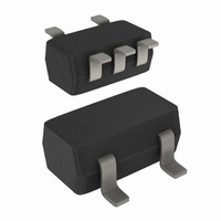
74AHCT1G00GW,125 NXP Semiconductors, 74AHCT1G00GW,125 Datasheet - Page 3

74AHCT1G00GW,125
Manufacturer Part Number
74AHCT1G00GW,125
Description
IC GATE NAND 2INPUT 5-TSSOP
Manufacturer
NXP Semiconductors
Series
74AHCTr
Datasheet
1.74AHC1G00GW125.pdf
(11 pages)
Specifications of 74AHCT1G00GW,125
Number Of Circuits
1
Package / Case
SC-70-5, SC-88A, SOT-323-5, SOT-353, 5-TSSOP
Logic Type
NAND Gate
Number Of Inputs
2
Current - Output High, Low
8mA, 8mA
Voltage - Supply
4.5 V ~ 5.5 V
Operating Temperature
-40°C ~ 125°C
Mounting Type
Surface Mount
Product
NAND
Logic Family
74AHC
High Level Output Current
- 8 mA
Low Level Output Current
8 mA
Propagation Delay Time
3.6 ns
Supply Voltage (max)
5.5 V
Supply Voltage (min)
4.5 V
Maximum Operating Temperature
+ 125 C
Mounting Style
SMD/SMT
Minimum Operating Temperature
- 40 C
Operating Temperature Range
- 40 C to + 125 C
Output Current
25 mA
Power Dissipation
250 mW
Lead Free Status / RoHS Status
Lead free / RoHS Compliant
Lead Free Status / RoHS Status
Lead free / RoHS Compliant, Lead free / RoHS Compliant
Other names
568-4826-2
74AHCT1G00GW,125
74AHCT1G00GW-G
74AHCT1G00GW-G
935262749125
74AHCT1G00GW,125
74AHCT1G00GW-G
74AHCT1G00GW-G
935262749125
Available stocks
Company
Part Number
Manufacturer
Quantity
Price
Company:
Part Number:
74AHCT1G00GW,125
Manufacturer:
PHI
Quantity:
100
NXP Semiconductors
7. Functional description
Table 4.
H = HIGH voltage level; L = LOW voltage level
8. Limiting values
Table 5.
In accordance with the Absolute Maximum Rating System (IEC 60134).
[1]
[2]
9. Recommended operating conditions
Table 6.
Voltages are referenced to GND (ground = 0 V).
74AHC_AHCT1G00_6
Product data sheet
Inputs
A
L
L
H
H
Symbol
V
V
I
I
I
I
I
T
P
Symbol Parameter
V
V
V
T
IK
OK
O
CC
GND
stg
amb
t/ V
CC
I
tot
CC
I
O
The input and output voltage ratings may be exceeded if the input and output current ratings are observed.
For both TSSOP5 and SC-74A packages: above 87.5 C the value of P
supply voltage
input voltage
output voltage
ambient temperature
input transition rise
and fall rate
Function table
Limiting values
Recommended operating conditions
Parameter
supply voltage
input voltage
input clamping current
output clamping current
output current
supply current
ground current
storage temperature
total power dissipation
Conditions
V
V
CC
CC
= 3.3 V
= 5.0 V
B
L
H
L
H
Conditions
V
V
T
0.5 V < V
I
O
amb
< 0.5 V
< 0.5 V or V
= 40 C to +125 C
0.3 V
0.5 V
Rev. 06 — 30 May 2007
O
< V
CC
74AHC1G00; 74AHCT1G00
O
> V
Min
+ 0.5 V
2.0
0
0
40
-
-
CC
tot
74AHC1G00
+ 0.5 V
derates linearly with 4.0 mW/K.
Typ
+25
5.0
-
-
-
-
+125
Max
V
100
5.5
5.5
20
CC
Output
Y
H
H
H
L
[1]
[2]
Min
4.5
Min
-
-
-
-
0
0
40
-
-
0.5
0.5
20
75
65
74AHCT1G00
Typ
+25
5.0
-
-
-
-
2-input NAND gate
Max
+7.0
+7.0
-
75
-
+150
250
© NXP B.V. 2007. All rights reserved.
20
25
+125
Max
V
5.5
5.5
20
CC
-
Unit
V
V
mA
mA
mA
mA
mA
mW
C
Unit
V
V
V
ns/V
ns/V
C
3 of 11


