74LVC06APW,118 NXP Semiconductors, 74LVC06APW,118 Datasheet - Page 3
74LVC06APW,118
Manufacturer Part Number
74LVC06APW,118
Description
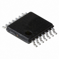
IC INVERTER HEX 1INPUT 14TSSOP
Manufacturer
NXP Semiconductors
Series
74LVCr
Datasheet
1.74LVC06AD118.pdf
(14 pages)
Specifications of 74LVC06APW,118
Package / Case
14-TSSOP
Logic Type
Inverter with Open Drain
Number Of Inputs
1
Number Of Circuits
6
Current - Output High, Low
32mA, 32mA
Voltage - Supply
1.65 V ~ 5.5 V
Operating Temperature
-40°C ~ 125°C
Mounting Type
Surface Mount
Logic Family
LVC
Number Of Channels Per Chip
6
Polarity
Inverting
Supply Voltage (max)
5.5 V
Supply Voltage (min)
1.65 V
Maximum Operating Temperature
+ 125 C
Mounting Style
SMD/SMT
Input Bias Current (max)
10 uA
Low Level Output Current
32 mA
Minimum Operating Temperature
- 40 C
Output Type
Open Drain
Propagation Delay Time
2.3 ns (Typ) @ 3.3 V
Number Of Lines (input / Output)
6 / 6
Logical Function
Buffer/Driver
Number Of Elements
6
Number Of Channels
6
Number Of Outputs
6
Operating Supply Voltage (typ)
1.8/2.5/3.3/5V
Package Type
TSSOP
Operating Supply Voltage (max)
5.5V
Operating Supply Voltage (min)
1.65V
Quiescent Current
10uA
Technology
CMOS
Pin Count
14
Mounting
Surface Mount
Operating Temp Range
-40C to 125C
Operating Temperature Classification
Automotive
Lead Free Status / RoHS Status
Lead free / RoHS Compliant
Lead Free Status / RoHS Status
Lead free / RoHS Compliant, Lead free / RoHS Compliant
Other names
568-4490-2
74LVC06APW-T
74LVC06APW-T
935265480118
74LVC06APW-T
74LVC06APW-T
935265480118
Available stocks
Company
Part Number
Manufacturer
Quantity
Price


Philips Semiconductors
ORDERING INFORMATION
PINNING
2003 Nov 27
handbook, halfpage
74LVC06AD
74LVC06APW
74LVC06ABQ
Hex inverter with open-drain outputs
Fig.1 Pin configuration (SO14 and TSSOP14).
TYPE NUMBER
PIN
10
11
12
13
14
1
2
3
4
5
6
7
8
9
GND
1A
1Y
2A
2Y
3A
3Y
1
2
3
4
5
6
7
06
MNA524
1A
1Y
2A
2Y
3A
3Y
GND
4Y
4A
5Y
5A
6Y
6A
V
TEMPERATURE RANGE
CC
14
13
12
11
10
9
8
40 to +125 C
40 to +125 C
40 to +125 C
V CC
6A
6Y
5A
5Y
4A
4Y
SYMBOL
3
data input
data output
data input
data output
data input
data output
ground (0 V)
data output
data input
data output
data input
data output
data input
supply voltage
handbook, halfpage
PINS
(1) The die substrate is attached to this pad using conductive die
14
14
14
attach material. It can not be used as a supply pin or input.
PACKAGE
Fig.2 Pin configuration (DHVQFN14).
1Y
2A
2Y
3A
3Y
DHVQFN14
PACKAGE
Top view
TSSOP14
2
3
4
5
6
SO14
DESCRIPTION
GND
1A
7
1
GND
V CC
MATERIAL
(1)
4Y
14
8
plastic
plastic
plastic
Product specification
MBL760
74LVC06A
13
12
11
10
9
6A
6Y
5A
5Y
4A
SOT108-1
SOT402-1
SOT762-1
CODE
Related parts for 74LVC06APW,118
Image
Part Number
Description
Manufacturer
Datasheet
Request
R

Part Number:
Description:
NXP Semiconductors designed the LPC2420/2460 microcontroller around a 16-bit/32-bitARM7TDMI-S CPU core with real-time debug interfaces that include both JTAG andembedded trace
Manufacturer:
NXP Semiconductors
Datasheet:

Part Number:
Description:
NXP Semiconductors designed the LPC2458 microcontroller around a 16-bit/32-bitARM7TDMI-S CPU core with real-time debug interfaces that include both JTAG andembedded trace
Manufacturer:
NXP Semiconductors
Datasheet:
Part Number:
Description:
NXP Semiconductors designed the LPC2468 microcontroller around a 16-bit/32-bitARM7TDMI-S CPU core with real-time debug interfaces that include both JTAG andembedded trace
Manufacturer:
NXP Semiconductors
Datasheet:
Part Number:
Description:
NXP Semiconductors designed the LPC2470 microcontroller, powered by theARM7TDMI-S core, to be a highly integrated microcontroller for a wide range ofapplications that require advanced communications and high quality graphic displays
Manufacturer:
NXP Semiconductors
Datasheet:
Part Number:
Description:
NXP Semiconductors designed the LPC2478 microcontroller, powered by theARM7TDMI-S core, to be a highly integrated microcontroller for a wide range ofapplications that require advanced communications and high quality graphic displays
Manufacturer:
NXP Semiconductors
Datasheet:
Part Number:
Description:
The Philips Semiconductors XA (eXtended Architecture) family of 16-bit single-chip microcontrollers is powerful enough to easily handle the requirements of high performance embedded applications, yet inexpensive enough to compete in the market for hi
Manufacturer:
NXP Semiconductors
Datasheet:
Part Number:
Description:
The XA-S3 device is a member of Philips Semiconductors? XA(eXtended Architecture) family of high performance 16-bitsingle-chip microcontrollers
Manufacturer:
NXP Semiconductors
Datasheet:

Part Number:
Description:
The NXP BlueStreak LH75401/LH75411 family consists of two low-cost 16/32-bit System-on-Chip (SoC) devices
Manufacturer:
NXP Semiconductors
Datasheet:
Part Number:
Description:
The NXP LPC3130/3131 combine an 180 MHz ARM926EJ-S CPU core, high-speed USB2
Manufacturer:
NXP Semiconductors
Datasheet:
Part Number:
Description:
The NXP LPC3141 combine a 270 MHz ARM926EJ-S CPU core, High-speed USB 2
Manufacturer:
NXP Semiconductors
Part Number:
Description:
The NXP LPC3143 combine a 270 MHz ARM926EJ-S CPU core, High-speed USB 2
Manufacturer:
NXP Semiconductors

Part Number:
Description:
The NXP LPC3152 combines an 180 MHz ARM926EJ-S CPU core, High-speed USB 2
Manufacturer:
NXP Semiconductors
Part Number:
Description:
The NXP LPC3154 combines an 180 MHz ARM926EJ-S CPU core, High-speed USB 2
Manufacturer:
NXP Semiconductors

Part Number:
Description:
Standard level N-channel enhancement mode Field-Effect Transistor (FET) in a plastic package using NXP High-Performance Automotive (HPA) TrenchMOS technology
Manufacturer:
NXP Semiconductors
Datasheet: