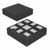
74AUP2G00GM,125 NXP Semiconductors, 74AUP2G00GM,125 Datasheet - Page 2

74AUP2G00GM,125
Manufacturer Part Number
74AUP2G00GM,125
Description
IC NAND GATE DL 2IN 8-XQFN
Manufacturer
NXP Semiconductors
Series
74AUPr
Datasheet
1.74AUP2G00DC125.pdf
(21 pages)
Specifications of 74AUP2G00GM,125
Number Of Circuits
2
Package / Case
8-XQFN
Logic Type
NAND Gate
Number Of Inputs
2
Current - Output High, Low
4mA, 4mA
Voltage - Supply
0.8 V ~ 3.6 V
Operating Temperature
-40°C ~ 125°C
Mounting Type
Surface Mount
Logic Family
AUP
High Level Output Current
- 4 mA
Low Level Output Current
4 mA
Propagation Delay Time
20.1 ns
Supply Voltage (max)
3.6 V
Supply Voltage (min)
0.8 V
Maximum Operating Temperature
+ 125 C
Mounting Style
SMD/SMT
Minimum Operating Temperature
- 40 C
Lead Free Status / RoHS Status
Lead free / RoHS Compliant
Lead Free Status / RoHS Status
Lead free / RoHS Compliant, Lead free / RoHS Compliant
Other names
74AUP2G00GM-G
74AUP2G00GM-G
935281423125
74AUP2G00GM-G
935281423125
NXP Semiconductors
3. Ordering information
Table 1.
4. Marking
Table 2.
[1]
5. Functional diagram
74AUP2G00
Product data sheet
Type number
74AUP2G00DC
74AUP2G00GT
74AUP2G00GF
74AUP2G00GD
74AUP2G00GM
74AUP2G00GN
74AUP2G00GS
Type number
74AUP2G00DC
74AUP2G00GT
74AUP2G00GF
74AUP2G00GD
74AUP2G00GM
74AUP2G00GN
74AUP2G00GS
Fig 1.
The pin 1 indicator is located on the lower left corner of the device, below the marking code.
Logic symbol
Ordering information
Marking codes
1A
1B
2A
2B
001aah748
Package
Temperature range Name
−40 °C to +125 °C
−40 °C to +125 °C
−40 °C to +125 °C
−40 °C to +125 °C
−40 °C to +125 °C
−40 °C to +125 °C
−40 °C to +125 °C
1Y
2Y
All information provided in this document is subject to legal disclaimers.
Fig 2.
VSSOP8 plastic very thin shrink small outline package; 8 leads;
XSON8
XSON8
XSON8U plastic extremely thin small outline package; no leads;
XQFN8U plastic extremely thin quad flat package; no leads;
XSON8
XSON8
Rev. 5 — 21 October 2010
IEC logic symbol
plastic extremely thin small outline package; no leads;
extremely thin small outline package; no leads;
extremely thin small outline package; no leads;
extremely thin small outline package; no leads;
Description
body width 2.3 mm
8 terminals; body 1 × 1.95 × 0.5 mm
8 terminals; body 1.35 × 1 × 0.5 mm
8 terminals; UTLP based; body 3 × 2 × 0.5 mm
8 terminals; UTLP based; body 1.6 × 1.6 × 0.5 mm
8 terminals; body 1.2 × 1.0 × 0.35 mm
8 terminals; body 1.35 × 1.0 × 0.35 mm
001aah749
&
&
Marking code
p00
p00
pA
p00
p00
pA
pA
[1]
Low-power dual 2-input NAND gate
Fig 3.
B
A
Logic diagram (one gate)
74AUP2G00
© NXP B.V. 2010. All rights reserved.
Version
SOT765-1
SOT833-1
SOT1089
SOT996-2
SOT902-1
SOT1116
SOT1203
mna099
2 of 21
Y


