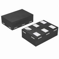
74AUP1G08GF,132 NXP Semiconductors, 74AUP1G08GF,132 Datasheet - Page 9

74AUP1G08GF,132
Manufacturer Part Number
74AUP1G08GF,132
Description
IC GATE AND 2-IN LP 6-XSON
Manufacturer
NXP Semiconductors
Series
74AUPr
Datasheet
1.74AUP1G08GW125.pdf
(20 pages)
Specifications of 74AUP1G08GF,132
Number Of Circuits
1
Package / Case
6-XSON, SOT891
Logic Type
AND Gate
Number Of Inputs
2
Current - Output High, Low
4mA, 4mA
Voltage - Supply
0.8 V ~ 3.6 V
Operating Temperature
-40°C ~ 125°C
Mounting Type
Surface Mount
Logic Family
AUP
High Level Output Current
- 4 mA
Low Level Output Current
4 mA
Propagation Delay Time
19.4 ns
Supply Voltage (max)
3.6 V
Supply Voltage (min)
0.8 V
Maximum Operating Temperature
+ 125 C
Mounting Style
SMD/SMT
Minimum Operating Temperature
- 40 C
Lead Free Status / RoHS Status
Lead free / RoHS Compliant
Lead Free Status / RoHS Status
Lead free / RoHS Compliant, Lead free / RoHS Compliant
Other names
74AUP1G08GF-H
74AUP1G08GF-H
935281109132
74AUP1G08GF-H
935281109132
NXP Semiconductors
Table 8.
Voltages are referenced to GND (ground = 0 V); for test circuit see
[1]
[2]
[3]
Table 9.
Voltages are referenced to GND (ground = 0 V); for test circuit see
74AUP1G08
Product data sheet
Symbol
T
C
Symbol
C
t
C
t
pd
pd
amb
PD
L
L
= 5 pF
= 10 pF
All typical values are measured at nominal V
t
C
P
f
f
C
V
N = number of inputs switching;
Σ(C
pd
i
o
D
CC
= 25 °C
PD
= input frequency in MHz;
L
= output frequency in MHz;
is the same as t
= output load capacitance in pF;
= C
L
is used to determine the dynamic power dissipation (P
= supply voltage in V;
× V
PD
Dynamic characteristics
Dynamic characteristics
CC
Parameter
power dissipation capacitance f = 1 MHz; V
Parameter
propagation delay
propagation delay
× V
2
× f
CC
o
2
) = sum of the outputs.
× f
PLH
i
× N + Σ(C
and t
PHL
L
.
× V
Conditions
A, B to Y; see
A, B to Y; see
CC
V
V
V
V
V
V
V
V
V
V
CC
CC
CC
CC
CC
CC
CC
CC
CC
CC
2
…continued
× f
= 1.1 V to 1.3 V
= 1.4 V to 1.6 V
= 1.65 V to 1.95 V
= 2.3 V to 2.7 V
= 3.0 V to 3.6 V
= 1.1 V to 1.3 V
= 1.4 V to 1.6 V
= 1.65 V to 1.95 V
= 2.3 V to 2.7 V
= 3.0 V to 3.6 V
o
All information provided in this document is subject to legal disclaimers.
) where:
CC
Conditions
.
V
V
V
V
V
V
CC
CC
CC
CC
CC
CC
Figure 7
Figure 7
Rev. 3 — 7 October 2010
= 0.8 V
= 1.1 V to 1.3 V
= 1.4 V to 1.6 V
= 1.65 V to 1.95 V
= 2.3 V to 2.7 V
= 3.0 V to 3.6 V
D
I
= GND to V
in μW).
[1]
[1]
Figure 8
Figure 8
CC
−40 °C to +85 °C
Min
2.1
2.2
1.5
1.3
1.0
0.9
1.8
1.6
1.3
1.2
[3]
Min
-
-
-
-
-
-
Max
13.6
11.7
7.5
6.1
4.8
4.3
8.9
7.2
5.7
4.7
Low-power 2-input AND gate
Typ
2.5
2.7
2.8
2.9
3.5
4.0
−40 °C to +125 °C
Min
74AUP1G08
2.1
1.5
1.3
1.0
0.9
2.2
1.8
1.6
1.3
1.2
[1]
Max
-
-
-
-
-
-
© NXP B.V. 2010. All rights reserved.
Max
12.9
15.0
8.3
6.7
5.3
4.8
9.8
7.9
6.3
5.2
Unit
pF
pF
pF
pF
pF
pF
Unit
ns
ns
ns
ns
ns
ns
ns
ns
ns
ns
9 of 20


