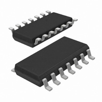
HEF4007UBT,653 NXP Semiconductors, HEF4007UBT,653 Datasheet - Page 8

HEF4007UBT,653
Manufacturer Part Number
HEF4007UBT,653
Description
IC DUAL PAIR/INVERTER 14SOIC
Manufacturer
NXP Semiconductors
Series
4000Br
Specifications of HEF4007UBT,653
Package / Case
14-SOIC (3.9mm Width), 14-SOL
Logic Type
Configurable Multiple Function
Number Of Circuits
2
Number Of Inputs
1
Mounting Type
Surface Mount
Logic Family
HEF4000
Number Of Channels Per Chip
3
Polarity
Inverting
Supply Voltage (max)
15.5 V
Supply Voltage (min)
4.5 V
Maximum Operating Temperature
+ 85 C
Mounting Style
SMD/SMT
High Level Output Current
- 3.6 mA (Min)
Input Bias Current (max)
4 uA
Low Level Output Current
3.6 mA (Min)
Minimum Operating Temperature
- 40 C
Propagation Delay Time
80 ns @ 5 V or 40 ns @ 10 V or 30 ns @ 15 V
Number Of Lines (input / Output)
3 / 3
Lead Free Status / RoHS Status
Lead free / RoHS Compliant
Voltage - Supply
-
Operating Temperature
-
Output Type
-
Current - Output High, Low
-
Schmitt Trigger Input
-
Lead Free Status / Rohs Status
Lead free / RoHS Compliant
Other names
933372620653
HEF4007UBTD-T
HEF4007UBTD-T
HEF4007UBTD-T
HEF4007UBTD-T
Philips Semiconductors
January 1995
Dual complementary pair and inverter
Fig.14 High impedance buffer.
8
FUNCTION TABLE for Fig.14.
Notes
1. H = HIGH state (the more positive voltage)
NOTE
Rules for maintaining electrical isolation between
transistors and monolithic substrate:
Violation of these rules will result in improper transistor
operation and/or possible permanent damage to the
HEF4007UB.
Pin number 14 must be maintained at the most positive
(or equally positive) potential with respect to any other
pin of the HEF4007UB.
Pin number 7 must be maintained at the most negative
(or equally negative) potential with respect to any other
pin of the HEF4007UB.
L = LOW state (the less positive voltage)
X = state is immaterial
INPUT
H
X
L
DISABLE
H
L
L
HEF4007UB
Product specification
OUTPUT
open
gates
H
L


