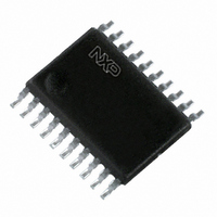
74LVC373APW,112 NXP Semiconductors, 74LVC373APW,112 Datasheet - Page 2

74LVC373APW,112
Manufacturer Part Number
74LVC373APW,112
Description
IC OCTAL D TRANSP LATCH 20TSSOP
Manufacturer
NXP Semiconductors
Series
74LVCr
Datasheet
1.74LVC373APW118.pdf
(20 pages)
Specifications of 74LVC373APW,112
Logic Type
D-Type Transparent Latch
Circuit
8:8
Output Type
Tri-State
Voltage - Supply
2.7 V ~ 3.6 V
Independent Circuits
1
Delay Time - Propagation
1.5ns
Current - Output High, Low
24mA, 24mA
Operating Temperature
-40°C ~ 125°C
Mounting Type
Surface Mount
Package / Case
20-TSSOP
Lead Free Status / RoHS Status
Lead free / RoHS Compliant
Other names
74LVC373APW
74LVC373APW
935218650112
74LVC373APW
935218650112
Philips Semiconductors
FEATURES
DESCRIPTION
The 74LVC373A is a high-performance, low-power,
low-voltage, Si-gate CMOS device, superior to most
advanced CMOS compatible TTL families.
Inputs can be driven from either 3.3 or 5 V devices.
In 3-state operation, outputs can handle 5 V. This feature
allows the use of these devices as translators in a mixed
3.3 and 5 V environment.
QUICK REFERENCE DATA
GND = 0 V; T
Notes
1. C
2. The condition is V
2003 May 19
t
C
C
PHL
5 V tolerant inputs/outputs for interfacing with 5 V logic
Wide supply voltage range from 1.2 to 3.6 V
CMOS low power consumption
Direct interface with TTL levels
Inputs accept voltages up to 5.5 V
High-impedance outputs when V
Complies with JEDEC standard no. 8-1A
ESD protection:
HBM EIA/JESD22-A114-A exceeds 2000 V
MM EIA/JESD22-A115-A exceeds 200 V
Specified from 40 to +85 C and 40 to +125 C.
I
PD
Octal D-type transparent latch with
5 V tolerant inputs/outputs; 3-state
P
f
f
C
V
N = total load switching outputs;
SYMBOL
i
o
/t
(C
D
CC
PD
= input frequency in MHz;
L
PLH
= output frequency in MHz;
= output load capacitance in pF;
= C
L
is used to determine the dynamic power dissipation (P
= supply voltage in Volts;
PD
V
CC
amb
2
V
CC
= 25 C; t
f
propagation delay
input capacitance
power dissipation capacitance per latch V
o
2
) = sum of the outputs.
Dn to Qn
LE to Qn
I
f
= GND to V
i
N + (C
r
= t
f
PARAMETER
2.5 ns.
L
CC
CC
.
= 0 V
V
CC
2
f
o
) where:
2
C
The 74LVC373A is an octal D-type transparent latch
featuring separate D-type inputs for each latch and 3-state
outputs for bus-oriented applications. A latch enable input
(pin LE) and an output enable input (pin OE) are common
to all internal latches.
The 74LVC373A consists of eight D-type transparent
latches with 3-state true outputs. When pin LE is HIGH,
data at the D-inputs (pins D0 to D7) enters the latches.
In this condition, the latches are transparent, i.e. a latch
output will change each time its corresponding D-input
changes. When pin LE is LOW, the latches store the
information that was present at the D-inputs one set-up
time preceding the HIGH-to-LOW transition of pin LE.
When pin OE is LOW, the contents of the eight latches are
available at the Q-outputs (pins Q0 to Q7). When pin OE is
HIGH, the outputs go to the high-impedance OFF-state.
Operation of input pin OE does not affect the state of the
latches.
The 74LVC373A is functionally identical to the
74LVC573A, but the 74LVC573A has a different pin
arrangement.
CC
L
D
= 50 pF; V
in W).
= 3.3 V; notes 1 and 2 14
CONDITIONS
CC
= 3.3 V
3.0
3.1
5.0
TYPICAL
Product specification
74LVC373A
ns
ns
pF
pF
UNIT


