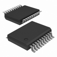
74LVC573ADB,118 NXP Semiconductors, 74LVC573ADB,118 Datasheet - Page 11

74LVC573ADB,118
Manufacturer Part Number
74LVC573ADB,118
Description
IC OCTAL D TRANSP LATCH 20SSOP
Manufacturer
NXP Semiconductors
Series
74LVCr
Datasheet
1.74LVC573APW118.pdf
(19 pages)
Specifications of 74LVC573ADB,118
Logic Type
D-Type Transparent Latch
Package / Case
20-SSOP
Circuit
8:8
Output Type
Tri-State
Voltage - Supply
2.7 V ~ 3.6 V
Independent Circuits
1
Delay Time - Propagation
1.5ns
Current - Output High, Low
24mA, 24mA
Operating Temperature
-40°C ~ 125°C
Mounting Type
Surface Mount
Number Of Circuits
8
Logic Family
LVC
Polarity
Non-Inverting
Input Bias Current (max)
0.1 uA
High Level Output Current
- 24 mA
Low Level Output Current
24 mA
Propagation Delay Time
3.4 ns at 3.3 V
Supply Voltage (max)
3.6 V
Supply Voltage (min)
1.2 V
Maximum Operating Temperature
+ 125 C
Minimum Operating Temperature
- 40 C
Mounting Style
SMD/SMT
Lead Free Status / RoHS Status
Lead free / RoHS Compliant
Lead Free Status / RoHS Status
Lead free / RoHS Compliant, Lead free / RoHS Compliant
Other names
74LVC573ADB-T
74LVC573ADB-T
935219010118
74LVC573ADB-T
935219010118
Philips Semiconductors
AC WAVEFORMS
2003 Oct 03
handbook, full pagewidth
Octal D-type transparent latch with 5 V
tolerant inputs/outputs; 3-state
V
V
V
V
V
V
M
M
OL
M
M
OL
= 1.5 V at V
= 0.5V
= 1.5 V at V
= 0.5V
and V
and V
Fig.8 Latch Enable input (LE) pulse width, the latch enable input to output (Qn) propagation delays.
CC
OH
CC
OH
are the typical output voltage drop that occur with the output load.
are the typical output voltage drop that occur with the output load.
at V
at V
CC
CC
CC
CC
< 2.7 V.
< 2.7 V.
2.7 V.
2.7 V.
Qn output
LE input
handbook, halfpage
Fig.7 Input (Dn) to output (Qn) propagation delays.
Qn output
Dn input
GND
V OH
V OL
V I
GND
V OH
V OL
V I
V M
t PHL
t W
1/f max
V M
V M
11
V M
t PHL
t PLH
MNA811
t PLH
MNA812
Product specification
74LVC573A


