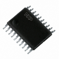
74LV573PW,118 NXP Semiconductors, 74LV573PW,118 Datasheet - Page 4

74LV573PW,118
Manufacturer Part Number
74LV573PW,118
Description
IC OCTAL D TRANSP LATCH 20TSSOP
Manufacturer
NXP Semiconductors
Series
74LVr
Type
D-Typer
Datasheet
1.74LV573N112.pdf
(18 pages)
Specifications of 74LV573PW,118
Logic Type
D-Type Transparent Latch
Package / Case
20-TSSOP
Circuit
8:8
Output Type
Tri-State
Voltage - Supply
1 V ~ 5.5 V
Independent Circuits
1
Delay Time - Propagation
24ns
Current - Output High, Low
16mA, 16mA
Operating Temperature
-40°C ~ 125°C
Mounting Type
Surface Mount
Number Of Circuits
8
Logic Family
LV
Polarity
Non-Inverting
High Level Output Current
- 16 mA
Low Level Output Current
16 mA
Propagation Delay Time
12 ns at 3.3 V
Supply Voltage (max)
5.5 V
Supply Voltage (min)
1 V
Maximum Operating Temperature
+ 125 C
Minimum Operating Temperature
- 40 C
Mounting Style
SMD/SMT
Number Of Bits
8
Number Of Elements
1
Latch Mode
Transparent
Technology
CMOS
Package Type
TSSOP
Operating Supply Voltage (typ)
3.3V
Operating Supply Voltage (min)
1V
Operating Supply Voltage (max)
5.5V
Operating Temp Range
-40C to 125C
Operating Temperature Classification
Automotive
Mounting
Surface Mount
Pin Count
20
Lead Free Status / RoHS Status
Lead free / RoHS Compliant
Lead Free Status / RoHS Status
Lead free / RoHS Compliant, Lead free / RoHS Compliant
Other names
74LV573PW-T
74LV573PW-T
935175070118
74LV573PW-T
935175070118
NXP Semiconductors
5. Pinning information
Table 2.
6. Functional description
Table 3.
[1]
74LV573_3
Product data sheet
Symbol
OE
D0 to D7
GND
LE
Q0 to Q7
V
Operating modes
Enable and read register
(transparent mode)
Latch and read register
Latch register and disable outputs
Fig 5.
CC
H = HIGH voltage level; h = HIGH voltage level one set-up time prior to the HIGH-to-LOW LE transition;
L = LOW voltage level; l = LOW voltage level one set-up time prior to the HIGH-to-LOW LE transition;
Z = high-impedance OFF-state.
Pin configuration DIP20, SO20
Pin description
Functional table
GND
OE
D0
D1
D2
D3
D4
D5
D6
D7
5.1 Pinning
5.2 Pin description
10
1
2
3
4
5
6
7
8
9
Pin
1
2, 3, 4, 5, 6, 7, 8, 9
10
11
19, 18, 17, 16, 15, 14, 13, 12
20
74LV573
[1]
001aaj966
20
19
18
17
16
15
14
13
12
11
Input
OE
L
L
L
L
H
H
V
Q0
Q1
Q2
Q3
Q4
Q5
Q6
Q7
LE
CC
Rev. 03 — 15 April 2009
Description
output enable input (active LOW)
data input
ground (0 V)
latch enable input (active HIGH)
data output
supply voltage
LE
H
H
L
L
L
L
Fig 6.
Pin configuration SSOP20, TSSOP20
Dn
L
H
l
h
l
h
GND
OE
D0
D1
D2
D3
D4
D5
D6
D7
Octal D-type transparent latch; 3-state
10
1
2
3
4
5
6
7
8
9
Internal latch Output
L
H
L
H
L
H
74LV573
001aaj967
© NXP B.V. 2009. All rights reserved.
74LV573
20
19
18
17
16
15
14
13
12
11
Qn
L
H
L
H
Z
Z
V
Q0
Q1
Q2
Q3
Q4
Q5
Q6
Q7
LE
CC
4 of 18


