74LVT162373DL,112 NXP Semiconductors, 74LVT162373DL,112 Datasheet - Page 2
74LVT162373DL,112
Manufacturer Part Number
74LVT162373DL,112
Description
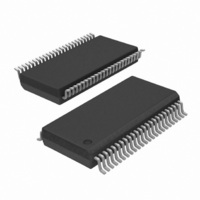
IC 16BIT TRANSP LATCH 48SSOP
Manufacturer
NXP Semiconductors
Series
74LVTr
Datasheet
1.74LVT162373DGG518.pdf
(12 pages)
Specifications of 74LVT162373DL,112
Logic Type
D-Type Transparent Latch
Circuit
8:8
Output Type
Tri-State
Voltage - Supply
2.7 V ~ 3.6 V
Independent Circuits
2
Delay Time - Propagation
3ns
Current - Output High, Low
12mA, 12mA
Operating Temperature
-40°C ~ 85°C
Mounting Type
Surface Mount
Package / Case
48-SSOP
Lead Free Status / RoHS Status
Lead free / RoHS Compliant
Other names
74LVT162373DL
74LVT162373DL
935264163112
74LVT162373DL
935264163112


FEATURES
QUICK REFERENCE DATA
ORDERING INFORMATION
Philips Semiconductors
1999 Sep 23
48-Pin Plastic SSOP Type III
48-Pin Plastic TSSOP Type II
16-bit transparent latch
3-State buffers
Output capability: +12 mA / –12 mA
TTL input and output switching levels
Input and output interface capability to systems at 5 V supply
Bus-hold data inputs eliminate the need for external pull-up
resistors to hold unused inputs
Live insertion/extraction permitted
Outputs include series resistance of 30
resistors unnecessary
Power-up reset
Power-up 3-State
No bus current loading when output is tied to 5 V bus
Latch-up protection exceeds 500 mA per JEDEC Std 17
ESD protection exceeds 2000 V per MIL STD 883 Method 3015
and 200 V per Machine Model
3.3 V LVT 16-bit transparent D-type latch
with 30
SYMBOL
C
I
t
t
C
PLH
PHL
CCZ
OUT
IN
PACKAGES
termination resistors (3-State)
Propagation delay
nDx to nQx
Input capacitance
Output capacitance
Total supply current
PARAMETER
making external
TEMPERATURE RANGE
–40 C to +85 C
–40 C to +85 C
C
V
V
Outputs disabled; V
Outputs disabled; V
L
CC
I
= 0 V or 3.0 V
= 50 pF;
= 3.3 V
2
DESCRIPTION
The 74LVT162373 is a high-performance BiCMOS product designed
for V
This device is a 16-bit transparent D-type latch with non-inverting
3-State bus compatible outputs. The device can be used as two
8-bit latches or one 16-bit latch. When Latch Enable (LE) input is
High, the Q outputs follow the data (D) inputs. When Latch Enable is
taken Low, the Q outputs are latched at the levels of the D inputs
one setup time prior to the High-to-Low transition.
The 74LVT162373 is designed with 30
the High and Low states of the output. This design reduces the
noise in applications such as memory address drivers, clock drivers,
and bus receivers/transmitters.
CONDITIONS
T
CC
amb
operation at 3.3 V.
= 25 C
O
CC
= 0 V or 3.0 V
74LVT162373 DGG
ORDERING CODE
= 3.6 V
74LVT162373 DL
TYPICAL
74LVT162373
series resistance in both
3.0
70
3
9
Product specification
DWG NUMBER
SOT370-1
SOT362-1
853-2172 22406
UNIT
ns
pF
pF
A
Related parts for 74LVT162373DL,112
Image
Part Number
Description
Manufacturer
Datasheet
Request
R

Part Number:
Description:
NXP Semiconductors designed the LPC2420/2460 microcontroller around a 16-bit/32-bitARM7TDMI-S CPU core with real-time debug interfaces that include both JTAG andembedded trace
Manufacturer:
NXP Semiconductors
Datasheet:

Part Number:
Description:
NXP Semiconductors designed the LPC2458 microcontroller around a 16-bit/32-bitARM7TDMI-S CPU core with real-time debug interfaces that include both JTAG andembedded trace
Manufacturer:
NXP Semiconductors
Datasheet:
Part Number:
Description:
NXP Semiconductors designed the LPC2468 microcontroller around a 16-bit/32-bitARM7TDMI-S CPU core with real-time debug interfaces that include both JTAG andembedded trace
Manufacturer:
NXP Semiconductors
Datasheet:
Part Number:
Description:
NXP Semiconductors designed the LPC2470 microcontroller, powered by theARM7TDMI-S core, to be a highly integrated microcontroller for a wide range ofapplications that require advanced communications and high quality graphic displays
Manufacturer:
NXP Semiconductors
Datasheet:
Part Number:
Description:
NXP Semiconductors designed the LPC2478 microcontroller, powered by theARM7TDMI-S core, to be a highly integrated microcontroller for a wide range ofapplications that require advanced communications and high quality graphic displays
Manufacturer:
NXP Semiconductors
Datasheet:
Part Number:
Description:
The Philips Semiconductors XA (eXtended Architecture) family of 16-bit single-chip microcontrollers is powerful enough to easily handle the requirements of high performance embedded applications, yet inexpensive enough to compete in the market for hi
Manufacturer:
NXP Semiconductors
Datasheet:
Part Number:
Description:
The XA-S3 device is a member of Philips Semiconductors? XA(eXtended Architecture) family of high performance 16-bitsingle-chip microcontrollers
Manufacturer:
NXP Semiconductors
Datasheet:

Part Number:
Description:
The NXP BlueStreak LH75401/LH75411 family consists of two low-cost 16/32-bit System-on-Chip (SoC) devices
Manufacturer:
NXP Semiconductors
Datasheet:
Part Number:
Description:
The NXP LPC3130/3131 combine an 180 MHz ARM926EJ-S CPU core, high-speed USB2
Manufacturer:
NXP Semiconductors
Datasheet:
Part Number:
Description:
The NXP LPC3141 combine a 270 MHz ARM926EJ-S CPU core, High-speed USB 2
Manufacturer:
NXP Semiconductors
Part Number:
Description:
The NXP LPC3143 combine a 270 MHz ARM926EJ-S CPU core, High-speed USB 2
Manufacturer:
NXP Semiconductors

Part Number:
Description:
The NXP LPC3152 combines an 180 MHz ARM926EJ-S CPU core, High-speed USB 2
Manufacturer:
NXP Semiconductors
Part Number:
Description:
The NXP LPC3154 combines an 180 MHz ARM926EJ-S CPU core, High-speed USB 2
Manufacturer:
NXP Semiconductors

Part Number:
Description:
Standard level N-channel enhancement mode Field-Effect Transistor (FET) in a plastic package using NXP High-Performance Automotive (HPA) TrenchMOS technology
Manufacturer:
NXP Semiconductors
Datasheet: