M74LCX16373DTR2G ON Semiconductor, M74LCX16373DTR2G Datasheet
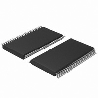
IC LATCH TRANSP 16BIT 48-TSSOP

M74LCX16373DTR2G

Manufacturer Part Number
M74LCX16373DTR2G
Description
IC LATCH TRANSP 16BIT 48-TSSOP
Manufacturer
ON Semiconductor
Series
74LCXr
Type
D-Typer
Datasheet

Specifications of M74LCX16373DTR2G

Logic Type
D-Type Transparent Latch
Circuit
8:8
Output Type
Tri-State
Voltage - Supply
2 V ~ 3.6 V
Independent Circuits
2
Delay Time - Propagation
1.5ns
Current - Output High, Low
24mA, 24mA
Operating Temperature
-55°C ~ 125°C
Mounting Type
Surface Mount
Package / Case
48-TSSOP
Logic Family
LCX
Number Of Bits
16
Number Of Elements
2
Latch Mode
Transparent
Polarity
Non-Inverting
Technology
CMOS
Package Type
TSSOP
Propagation Delay Time
7.9ns
Operating Supply Voltage (typ)
2.5/3.3V
High Level Output Current
-24mA
Low Level Output Current
24mA
Operating Supply Voltage (min)
2V
Operating Supply Voltage (max)
3.6V
Operating Temp Range
-55C to 125C
Operating Temperature Classification
Military
Mounting
Surface Mount
Pin Count
48
Lead Free Status / RoHS Status
Lead free / RoHS Compliant

Available stocks

Company
Part Number
Manufacturer
Quantity
Price
Part Number:
M74LCX16373DTR2G
Quantity:
5 000
Part Number:
M74LCX16373DTR2G
Manufacturer:
TEXAS
Quantity:
750
Part Number:
M74LCX16373DTR2G
Manufacturer:
ON/安森美
Quantity:
20 000
MC74LCX16373
Low-Voltage CMOS 16-Bit
Transparent Latch
With 5 V−Tolerant Inputs and Outputs
(3−State, Non−Inverting)
transparent latch operating from a 2.3 V to 3.6 V supply. The device is
byte controlled. Each byte has separate Output Enable and Latch Enable
inputs. These control pins can be tied together for full 16−bit operation.
High impedance TTL compatible inputs significantly reduce current
loading to input drivers while TTL compatible outputs offer improved
switching noise performance. A V
MC74LCX16373 inputs to be safely driven from 5.0 V devices.
5.0 V−tolerant outputs. When the Latch Enable (LEn) inputs are HIGH,
data on the Dn inputs enters the latches. In this condition, the latches are
transparent, i.e., a latch output will change state each time its D input
changes. When LE is LOW, the latches store the information that was
present on the D inputs a setup time preceding the HIGH−to−LOW
transition of LE. The 3−state outputs are controlled by the Output
Enable (OEn) inputs. When OE is LOW, the outputs are enabled. When
OE is HIGH, the standard outputs are in the high impedance state, but
this does not interfere with new data entering into the latches.
Features
*For additional information on our Pb−Free strategy and soldering details, please
© Semiconductor Components Industries, LLC, 2010
July, 2010 − Rev. 8
download the ON Semiconductor Soldering and Mounting Techniques
Reference Manual, SOLDERRM/D.
The MC74LCX16373 is a high performance, non−inverting 16−bit
The MC74LCX16373 contains 16 D−type latches with 3−state
Substantially Reduces System Power Requirements
Designed for 2.3 to 3.6 V V
5.4 ns Maximum t
5.0 V Tolerant − Interface Capability With 5.0 V TTL Logic
Supports Live Insertion and Withdrawal
I
LVTTL Compatible
LVCMOS Compatible
24 mA Balanced Output Sink and Source Capability
Near Zero Static Supply Current in All Three Logic States (20 mA)
Latchup Performance Exceeds 500 mA
ESD Performance: Human Body Model >2000 V;
These are Pb−Free Devices*
OFF
Specification Guarantees High Impedance When V
pd
Machine Model >200 V
CC
Operation
I
specification of 5.5 V allows
CC
1
= 0 V
See detailed ordering and shipping information in the package
dimensions section on page 3 of this data sheet.
48
ORDERING INFORMATION
A
WL
YY
WW
G
MARKING DIAGRAM
1
http://onsemi.com
48
1
LCX16373G
= Assembly Location
= Wafer Lot
= Year
= Work Week
= Pb−Free Package
AWLYYWW
Publication Order Number:
CASE 1201
DT SUFFIX
TSSOP−48
MC74LCX16373/D

Related parts for M74LCX16373DTR2G

M74LCX16373DTR2G Summary of contents

Page 1

... Machine Model >200 V • These are Pb−Free Devices* *For additional information on our Pb−Free strategy and soldering details, please download the ON Semiconductor Soldering and Mounting Techniques Reference Manual, SOLDERRM/D. © Semiconductor Components Industries, LLC, 2010 July, 2010 − Rev. 8 specification of 5.5 V allows ...

Page 2

OE1 LE1 GND GND ...

Page 3

... ORDERING INFORMATION Device MC74LCX16373DT MC74LCX16373DTG MC74LCX16373DTR2 M74LCX16373DTR2G †For information on tape and reel specifications, including part orientation and tape sizes, please refer to our Tape and Reel Packaging Specifications Brochure, BRD8011/D. *This package is inherently Pb−Free. MAXIMUM RATINGS Symbol Parameter V DC Supply Voltage Input Voltage ...

Page 4

DC ELECTRICAL CHARACTERISTICS Symbol Characteristic V HIGH Level Input Voltage (Note LOW Level Input Voltage (Note HIGH Level Output Voltage OH V LOW Level Output Voltage OL I Input Leakage Current I I 3−State ...

Page 5

DYNAMIC SWITCHING CHARACTERISTICS Symbol Characteristic V Dynamic LOW Peak Voltage OLP (Note 4) V Dynamic LOW Valley Voltage OLV (Note 4) 4. Number of outputs defined as “n”. Measured with “n−1” outputs switching from HIGH−to−LOW or LOW−to−HIGH. The remaining output ...

Page 6

PULSE GENERATOR R T Figure 4. Test Circuit Table 3. TEST CIRCUIT TEST PLH PHL PZL PLZ Open Collector/Drain t and t PLH PHL PZH PHZ ...

Page 7

... Opportunity/Affirmative Action Employer. This literature is subject to all applicable copyright laws and is not for resale in any manner. PUBLICATION ORDERING INFORMATION LITERATURE FULFILLMENT: Literature Distribution Center for ON Semiconductor P.O. Box 5163, Denver, Colorado 80217 USA Phone: 303−675−2175 or 800−344−3860 Toll Free USA/Canada Fax: 303− ...

Related keywords