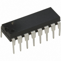
74F402PC Fairchild Semiconductor, 74F402PC Datasheet - Page 4

74F402PC
Manufacturer Part Number
74F402PC
Description
IC PARITY GEN/CHKER 16BIT 16DIP
Manufacturer
Fairchild Semiconductor
Series
74Fr
Datasheet
1.74F402PC.pdf
(9 pages)
Specifications of 74F402PC
Logic Type
Parity Generator/Checker
Number Of Circuits
16-Bit
Current - Output High, Low
5.7mA, 16mA
Voltage - Supply
4.5 V ~ 5.5 V
Operating Temperature
0°C ~ 70°C
Mounting Type
Through Hole
Package / Case
16-DIP (0.300", 7.62mm)
Lead Free Status / RoHS Status
Lead free / RoHS Compliant
Other names
74F402
Available stocks
Company
Part Number
Manufacturer
Quantity
Price
Part Number:
74F402PC
Manufacturer:
NS/ه›½هچٹ
Quantity:
20 000
www.fairchildsemi.com
Applications
In addition to polynomial selection there are four other
capabilities provided for in the 74F402 ROM. The first is set
or clear selectability. The sixteen internal registers have the
capability to be either set or cleared when P is brought
LOW. This set or clear capability is done in four groups of 4
(see Table 2, P
determining the polarity of the check word. As is the case
with the Ethernet polynomial the check word can be
inverted when it is appended to the data stream or as is the
case with the other polynomials, the residue is appended
with no inversion. Thirdly, the ROM contains a bit (C
which is used to select the RFB input instead of the SEI
input to be fed into the LSB. This is used when the polyno-
mial selected is actually a residue (least significant) stored
in the ROM which indicates whether the selected location
is a polynomial or a residue. If the latter, then it inhibits the
RFB input.
As mentioned previously, upon a successful data transmis-
sion, the CRC register has a zero residue. There is an
exception to this, however, with respect to the Ethernet
polynomial. This polynomial, upon a successful data trans-
mission, has a non-zero residue in the CRC register (C7 04
DD 7B)
ROM locations have been preloaded with the residue so
that by selecting these locations and clocking the device
one additional time, after the last check bit has been
entered, will result in zeroing the CRC register. In this man-
ner a no-error indication is achieved.
With the present mix of polynomials, the largest is 56
order requiring four devices while the smallest is 16
requiring just one device. In order to accommodate multi-
plexing between high order polynomials (X 16
lower order polynomials, a location of all zeros is provided.
16
. In order to provide a no-error indication, two
Select Code
0
–P
C
D
E
B
A
0
F
7
3
2
4
8
5
9
1
6
3
). The second ROM capability (C
P
0
1
1
0
0
1
1
1
1
1
0
1
1
1
1
1
3
P
0
1
1
0
0
1
1
1
1
1
0
1
1
1
1
1
2
th
order) and
th
P
0
1
1
0
0
1
1
1
1
1
1
1
1
1
1
1
0
1
) is in
order
TABLE 2.
1
th
)
P
4
0
1
1
0
0
1
1
1
1
1
1
1
1
1
1
1
0
This allows the user to choose a lower order polynomial
even if the system is configured for a higher order one.
The 74F402 expandable CRC generator checker contains
6 popular CRC polynomials, 2-16
48
shows the 74F402 connected for a 56
Also shown are the input patterns for other polynomials.
When the 74F402 is used with a gated clock, disabling the
clock in a HIGH state will ensure no erroneous clocking
occurs when the clock is re-enabled. Preset and Master
Reset are asynchronous inputs presetting the register to S
or clearing to 1s respectively (note Ethernet residue and
56
To generate a CRC, the pattern for the selected polynomial
is applied to the S inputs, the register is preset or cleared
as required, clock is enabled, CWG is set HIGH, data is
applied to D input, output data is on D/CW. When the last
data bit has been entered, CWG is set LOW and the regis-
ter is clocked for n bits (where n is the order of the polyno-
mial). The clock may now be stopped if desired (holding
CWG LOW and clocking the register will output zeros from
D/CW after the residue has been shifted out).
To check a CRC, the pattern for the selected polynomial is
applied to the S inputs, the register is preset or cleared as
required, clock is enabled, CWG is set HIGH, the data
stream including the CRC is applied to D input. When the
last bit of the CRC has been entered, the ER output is
checked: HIGH
clock may now be stopped if desired.
To implement polynomials of lower order than 56
the number of packages required for the order of polyno-
mial and apply the pattern for the selected polynomial to
the S inputs (0000 on S inputs disables the package from
the feedback chain).
th
th
Order select code 8, LSB, are exceptions to this).
Order and 1-56
C
1
1
1
0
0
1
1
1
1
1
1
1
1
1
1
1
2
C
0
0
0
0
1
0
0
0
0
0
0
0
0
0
0
0
error free data, LOW
1
th
Order. The application diagram
C
0
1
1
0
0
0
0
0
0
0
0
0
0
0
0
0
0
th
S
Ethernet
Polynomial
Ethernet
Residue
CRC-16
CRC-CCITT
56th
Order
48th
Order
32nd
Order
Order, 2-32
Polynomial
0
th
Order polynomial.
corrupt data. The
nd
Order, 1-
th
, select


