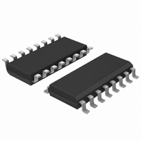
74HC4094D,653 NXP Semiconductors, 74HC4094D,653 Datasheet - Page 5

74HC4094D,653
Manufacturer Part Number
74HC4094D,653
Description
IC REGISTER BUS 8STAGE 16SOIC
Manufacturer
NXP Semiconductors
Series
74HCr
Type
Not Requiredr
Specifications of 74HC4094D,653
Package / Case
16-SOIC (3.9mm Width)
Logic Type
Shift Register
Output Type
Standard
Function
Serial to Parallel
Number Of Elements
1
Number Of Bits Per Element
8
Voltage - Supply
2 V ~ 6 V
Operating Temperature
-40°C ~ 125°C
Mounting Type
Surface Mount
Counting Sequence
Serial to Serial/Parallel
Number Of Circuits
1
Logic Family
HC
Propagation Delay Time
195 ns, 39 ns, 33 ns
Supply Voltage (max)
6 V
Maximum Operating Temperature
+ 125 C
Minimum Operating Temperature
- 40 C
Mounting Style
SMD/SMT
Technology
CMOS
Number Of Elements
1
Number Of Bits
8
Logical Function
Shift Register
Operating Supply Voltage (typ)
5V
Package Type
SO
Operating Temp Range
-40C to 125C
Operating Supply Voltage (min)
2V
Operating Supply Voltage (max)
6V
Operating Temperature Classification
Automotive
Mounting
Surface Mount
Pin Count
16
Lead Free Status / RoHS Status
Lead free / RoHS Compliant
Lead Free Status / RoHS Status
Lead free / RoHS Compliant, Lead free / RoHS Compliant
Other names
568-2265-2
74HC4094D-T
933714850653
74HC4094D-T
933714850653
NXP Semiconductors
7. Functional description
Table 3.
[1]
74HC_HCT4094
Product data sheet
Inputs
CP
↑
↓
↑
↑
↑
↓
Fig 7.
At the positive clock edge, the information in the 7th register stage is transferred to the 8th register stage and the QSn outputs.
H = HIGH voltage level; L = LOW voltage level; X = don’t care;
↑ = positive-going transition; ↓ = negative-going transition;
Z = HIGH-impedance OFF-state; NC = no change;
Q6S = the data in register stage 6 before the LOW to HIGH clock transition;
Q7S = the data in register stage 7 before the HIGH to LOW clock transition.
Timing diagram
Function table
OE
L
L
H
H
H
H
OUTPUT ENABLE INPUT
INTERNAL Q0S (FF 0)
INTERNAL Q6S (FF 6)
SERIAL OUTPUT QS1
SERIAL OUTPUT QS2
STROBE INPUT
CLOCK INPUT
OUTPUT QP0
OUTPUT QP6
DATA INPUT
[1]
STR
X
X
L
H
H
H
All information provided in this document is subject to legal disclaimers.
D
X
X
X
L
H
H
Rev. 3 — 14 February 2011
Parallel outputs
QP0
Z
Z
NC
L
H
NC
74HC4094; 74HCT4094
Z-state
Z-state
QPn
Z
Z
NC
QPn −1
QPn −1
NC
8-stage shift-and-store bus register
Serial outputs
QS1
Q6S
NC
Q6S
Q6S
Q6S
NC
001aaf117
© NXP B.V. 2011. All rights reserved.
QS2
NC
Q7S
NC
NC
NC
Q7S
5 of 23


