HEF4014BT,653 NXP Semiconductors, HEF4014BT,653 Datasheet
HEF4014BT,653
Specifications of HEF4014BT,653
HEF4014BTD-T
HEF4014BTD-T


Related parts for HEF4014BT,653


HEF4014BT,653 Summary of contents
Page 1
HEF4014B 8-bit static shift register Rev. 06 — 2 November 2009 1. General description The HEF4014B is a fully synchronous edge-triggered 8-bit static shift register with eight synchronous parallel inputs (D0 to D7), a synchronous serial data input (DS), a ...
Page 2
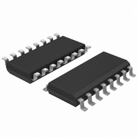
... NXP Semiconductors 4. Ordering information Table 1. Ordering information All types operate from +85 C Type number Package Name Description HEF4014BP DIP16 plastic dual in-line package; 16-leads (300 mil) HEF4014BT SO16 plastic small outline package; 16 leads; body width 3 Functional diagram Fig 1. Functional diagram Fig 2 ...
Page 3
... NXP Semiconductors 6. Pinning information 6.1 Pinning Fig 3. Pin configuration DIP16 and SO16 6.2 Pin description Table 2. Pin description Symbol Pin 12 13, 14, 15 HEF4014B_6 Product data sheet HEF4014B 001aae557 Description output parallel data input ground supply voltage parallel enable input clock input (LOW-to-HIGH edge-triggered) ...
Page 4
... NXP Semiconductors 7. Functional description [1] Table 3. Function table Number of clock Inputs transitions CP Serial operation Parallel operation 1 [ HIGH voltage level LOW voltage level don’t care HIGH or LOW; = LOW-to-HIGH clock transition; 8. Limiting values Table 4. Limiting values In accordance with the Absolute Maximum Rating System (IEC 60134). ...
Page 5
... NXP Semiconductors 9. Recommended operating conditions Table 5. Recommended operating conditions Symbol Parameter V supply voltage DD V input voltage I T ambient temperature amb t/ V input transition rise and fall rate 10. Static characteristics Table 6. Static characteristics unless otherwise specified Symbol Parameter V HIGH-level input voltage ...
Page 6
... NXP Semiconductors 11. Dynamic characteristics Table 7. Dynamic characteristics amb SS Symbol Parameter Conditions t HIGH to LOW CP to Qn; PHL propagation delay see t LOW to HIGH CP to Qn; PLH propagation delay see t transition time Qn output; t see t pulse width CP input; W minimum width; see t set-up time PE su see DS see Dn see ...
Page 7
... NXP Semiconductors Table 8. Dynamic power dissipation P P can be calculated from the formulas shown Symbol Parameter dynamic power dissipation 12. Waveforms Measurement points are given in Fig propagation delays and output transition times input input input input V SS The shaded areas indicate where change is permitted for predictable output performance. ...
Page 8
... NXP Semiconductors Table 9. Measurement points Supply voltage Test data is given in Table Definitions for test circuit: DUT = Device Under Test load capacitance including jig and probe capacitance termination resistance should be equal to the output impedance Z T Fig 6. Test circuit Table 10. Test data Supply voltage ...
Page 9
... NXP Semiconductors 13. Package outline DIP16: plastic dual in-line package; 16 leads (300 mil pin 1 index 1 DIMENSIONS (inch dimensions are derived from the original mm dimensions UNIT max. min. max. mm 4.2 0.51 3.2 inches 0.17 0.02 0.13 Note 1. Plastic or metal protrusions of 0.25 mm (0.01 inch) maximum per side are not included. ...
Page 10
... NXP Semiconductors SO16: plastic small outline package; 16 leads; body width 3 pin 1 index 1 DIMENSIONS (inch dimensions are derived from the original mm dimensions) A UNIT max. 0.25 1.45 mm 1.75 0.25 0.10 1.25 0.010 0.057 inches 0.069 0.01 0.004 0.049 Note 1. Plastic or metal protrusions of 0.15 mm (0.006 inch) maximum per side are not included. ...
Page 11
... NXP Semiconductors 14. Revision history Table 11. Revision history Document ID Release date HEF4014B_6 20091102 • Modifications: Section 9 “Recommended operating conditions” HEF4014B_5 20090624 HEF4014B_4 20090122 HEF4014B_CNV_3 19950101 HEF4014B_CNV_2 19950101 HEF4014B_6 Product data sheet Data sheet status Change notice Product data sheet - Product data sheet ...
Page 12
... Right to make changes — NXP Semiconductors reserves the right to make changes to information published in this document, including without limitation specifications and product descriptions, at any time and without notice ...
Page 13
... NXP Semiconductors 17. Contents 1 General description . . . . . . . . . . . . . . . . . . . . . . 1 2 Features . . . . . . . . . . . . . . . . . . . . . . . . . . . . . . . 1 3 Applications . . . . . . . . . . . . . . . . . . . . . . . . . . . . 1 4 Ordering information . . . . . . . . . . . . . . . . . . . . . 2 5 Functional diagram . . . . . . . . . . . . . . . . . . . . . . 2 6 Pinning information . . . . . . . . . . . . . . . . . . . . . . 3 6.1 Pinning . . . . . . . . . . . . . . . . . . . . . . . . . . . . . . . 3 6.2 Pin description . . . . . . . . . . . . . . . . . . . . . . . . . 3 7 Functional description . . . . . . . . . . . . . . . . . . . 4 8 Limiting values Recommended operating conditions Static characteristics Dynamic characteristics . . . . . . . . . . . . . . . . . . 6 12 Waveforms . . . . . . . . . . . . . . . . . . . . . . . . . . . . . 7 13 Package outline . . . . . . . . . . . . . . . . . . . . . . . . . 9 14 Revision history ...