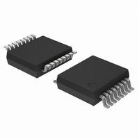
74LV595DB,118 NXP Semiconductors, 74LV595DB,118 Datasheet - Page 10

74LV595DB,118
Manufacturer Part Number
74LV595DB,118
Description
IC 8BIT SHIFT REGISTER 16SSOP
Manufacturer
NXP Semiconductors
Series
74LVr
Datasheet
1.74LV595DB118.pdf
(20 pages)
Specifications of 74LV595DB,118
Package / Case
16-SSOP
Logic Type
Shift Register
Output Type
Standard
Function
Serial to Parallel
Number Of Elements
1
Number Of Bits Per Element
8
Voltage - Supply
1 V ~ 3.6 V
Operating Temperature
-40°C ~ 125°C
Mounting Type
Surface Mount
Counting Sequence
Serial to Serial/Parallel
Number Of Circuits
1
Logic Family
LV
Propagation Delay Time
15 ns
Supply Voltage (max)
3.6 V
Maximum Operating Temperature
+ 125 C
Minimum Operating Temperature
- 40 C
Mounting Style
SMD/SMT
Supply Voltage (min)
1 V
Lead Free Status / RoHS Status
Lead free / RoHS Compliant
Lead Free Status / RoHS Status
Lead free / RoHS Compliant, Lead free / RoHS Compliant
Other names
74LV595DB-T
74LV595DB-T
935198280118
74LV595DB-T
935198280118
NXP Semiconductors
Table 7.
Voltages are referenced to GND (ground = 0 V). For test circuit see
[1]
[2]
[3]
[4]
[5]
[6]
[7]
12. Waveforms
74LV595_3
Product data sheet
Symbol Parameter
f
C
max
Fig 8.
PD
Typical values are measured at T
t
Typical value measured at V
t
t
Skew between any two outputs of the same package switching in the same direction. This parameter is guaranteed by design.
C
P
f
f
C
V
N = number of inputs switching;
pd
en
dis
i
o
D
CC
PD
= input frequency in MHz;
L
(C
= output frequency in MHz;
is the same as t
is the same as t
= output load capacitance in pF;
is the same as t
= C
L
is used to determine the dynamic power dissipation (P
= supply voltage in V;
maximum
frequency
power dissipation
capacitance
Measurement points are given in
V
The shift clock (SHCP) to serial data output (Q7S) propagation delays, the shift clock pulse width and
maximum shift clock frequency
PD
V
OL
Dynamic characteristics
CC
and V
2
V
CC
f
o
2
) = sum of outputs.
OH
PLH
PZH
f
PHZ
i
are typical output voltage drops that occur with the output load.
N + (C
and t
and t
and t
PHL
PZL
CC
PLZ
Conditions
SHCP or STCP; see
and
V
SH CP input
Q 7 S output
I
L
.
= 3.3 V.
.
.
V
V
V
V
= GND to V
amb
CC
CC
CC
CC
Figure 9
V
CC
= 2.0 V
= 2.7 V
= 3.3 V; C
= 3.0 V to 3.6 V
= 25 C.
…continued
2
GND
V
V
OH
Table
OL
V
f
I
o
) where:
CC;
8.
L
V
= 15 pF
CC
Rev. 03 — 21 April 2009
Figure 8
V
= 3.0 V
M
t
8-bit serial-in/serial-out or parallel-out shift register; 3-state
PLH
t
W
D
in W).
1/f
V
M
max
[3]
[7]
Figure
14.0
19.0
24.0
Min
-
-
40 C to +85 C
13.
t
Typ
PHL
40.0
58.0
70.0
115
77
[1]
mna557
Max
-
-
-
-
-
40 C to +125 C
Min
12
16
20
-
-
© NXP B.V. 2009. All rights reserved.
74LV595
Max
-
-
-
-
-
10 of 20
Unit
MHz
MHz
MHz
MHz
pF


