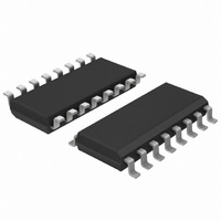
N74F194D,623 NXP Semiconductors, N74F194D,623 Datasheet - Page 5

N74F194D,623
Manufacturer Part Number
N74F194D,623
Description
IC SHIFT REGISTER 4BIT 16SOIC
Manufacturer
NXP Semiconductors
Series
74Fr
Datasheet
1.N74F194D623.pdf
(10 pages)
Specifications of N74F194D,623
Logic Type
Register, Bidirectional
Output Type
Standard
Number Of Elements
1
Number Of Bits Per Element
4
Function
Universal
Voltage - Supply
4.5 V ~ 5.5 V
Operating Temperature
0°C ~ 70°C
Mounting Type
Surface Mount
Package / Case
16-SOIC (3.9mm Width)
Lead Free Status / RoHS Status
Lead free / RoHS Compliant
Other names
933784230623
N74F194D-T
N74F194D-T
N74F194D-T
N74F194D-T
1. For conditions shown as MIN or MAX, use the appropriate value specified under recommended operating conditions for the applicable type.
2. All typical values are at V
3. Output High state will change to Low stat if an external voltage of less than 0.0V is applied.
4. Not more than one output should be shorted at a time. For testing I
5. With all outputs open, D
Philips Semiconductors
DC ELECTRICAL CHARACTERISTICS
NOTES:
AC ELECTRICAL CHARACTERISTICS
AC SETUP REQUIREMENTS
April 4, 1989
V
V
V
V
V
I
I
I
I
I
SYMBOL
SYMBOL
I
IH
IL
OS
CC
SYMBOL
SYMBOL
f
t
t
t
t
t
t
t
t
t
t
t
t
t
t
O
OH
O
OL
IK
MAX
PLH
PHL
PHL
S
S
h
h
S
S
h
h
W
W
REC
4-bit bidirectional universal shift register
techniques are preferable in order to minimize internal heating and more accurately reflect operational values. Otherwise, prolonged shorting
of a High output may raise the chip temperature well above normal and thereby cause invalid readings in other parameter tests. In any
sequence of parameter tests, I
then 4.5V applied to CP.
(H)
(L)
(H)
(L)
(H)
(L)
(H)
(L)
(H)
(L)
High level output voltage
High-level output voltage
Low level output voltage
Low-level output voltage
Input clamp voltage
Input current at maximum input voltage
High-level input current
Low-level input current
Short-circuit output current
Supply current (total)
Propagation delay
CP to Qn
Propagation delay
MR to Qn
Maximum clock frequency
Setup time, High or Low
Dn, D
Hold time, High or Low
Dn, D
Setup time, High or Low
Sn to CP
Hold time, High or Low
Sn to CP
CP Pulse width, High
MR Pulse width, Low
Recovery time, MR to CP
SL
SL
, D
, D
SR
SR
PARAMETER
PARAMETER
i
inputs grounded and a 4.5V applied to S0, S1, MR and the serial inputs, I
CC
to CP
to CP
PARAMETER
PARAMETER
= 5V, T
OS
5
tests should be performed last.
amb
3
3
4
= 25 C.
CONDITION
CONDITION
Waveform 1
Waveform 1
Waveform 2
Waveform 3
Waveform 3
Waveform 3
Waveform 3
Waveform 1
Waveform 2
Waveform 2
V
V
V
V
V
V
V
V
V
V
TEST
TEST
CC
IH
CC
IH
CC
CC
CC
CC
CC
CC
= MIN, I
= MIN, I
= MIN, V
= MIN, V
= MIN, I
= MAX, V
= MAX, V
= MAX, V
= MAX
= MAX
TEST CONDITIONS
TEST CONDITIONS
OS
5
, the use of high-speed test apparatus and/or sample-and-hold
OH
OL
I
IL
IL
= I
I
I
I
= MAX
= MAX
= 7.0V
= 2.7V
= 0.5V
= MAX
= MAX
C
C
MIN
MIN
IK
105
3.5
3.5
4.5
4.0
4.0
8.0
8.0
5.0
5.0
7.0
L
L
0
0
0
0
= 50pF, R
= 50pF, R
T
T
V
V
amb
amb
CC
CC
TYP
TYP
150
= +5.0V
5.2
5.5
8.6
= +5.0V
= +25 C
= +25 C
10%V
10%V
5%V
5%V
1
1
L
L
= 500
= 500
CC
CC
CC
CC
MAX
MAX
12.0
7.0
7.0
LIMITS
LIMITS
CC
MIN
–60
2.5
2.7
is tested with a momentary ground,
C
C
T
T
V
V
L
L
amb
amb
MIN
MIN
CC
3.5
3.5
4.5
CC
4.0
4.0
1.0
1.0
9.0
8.0
5.5
5.0
8.0
90
= 50pF, R
= 50pF, R
0
0
LIMITS
= +5.0V
= +5.0V
= 0 C to +70 C
= 0 C to +70 C
TYP
–0.73
0.30
0.30
3.4
33
2
L
L
= 500
= 500
MAX
MAX
14.0
10%
8.0
8.0
10%
MAX
–150
0.50
0.50
–1.2
–0.6
100
Product specification
20
46
74F194
UNIT
UNIT
UNIT
UNIT
MHz
mA
mA
mA
ns
ns
ns
ns
ns
ns
ns
ns
ns
V
V
V
V
V
A
A


